Semiconductor device

A semiconductor, planar technology, used in semiconductor devices, semiconductor/solid-state device manufacturing, semiconductor/solid-state device components, etc.

Inactive Publication Date: 2004-01-28
INFINEON TECH AG
View PDF1 Cites 0 Cited by
  • Summary
  • Abstract
  • Description
  • Claims
  • Application Information

AI Technical Summary

Problems solved by technology

But in this way, the electrons brought into the nitride layer after this heating cannot be removed by another heating step.

Method used


Image

  • Semiconductor device
  • Semiconductor device
  • Semiconductor device

Examples


Embodiment Construction

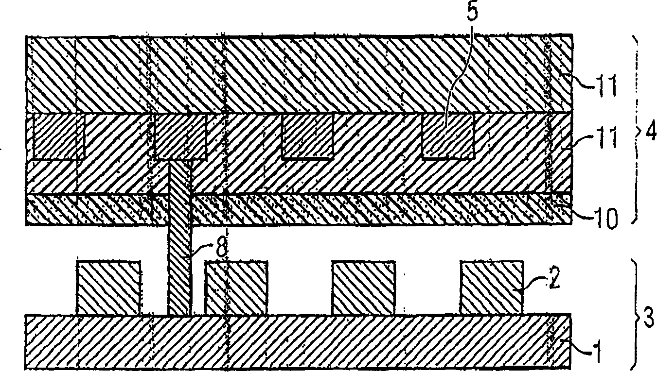
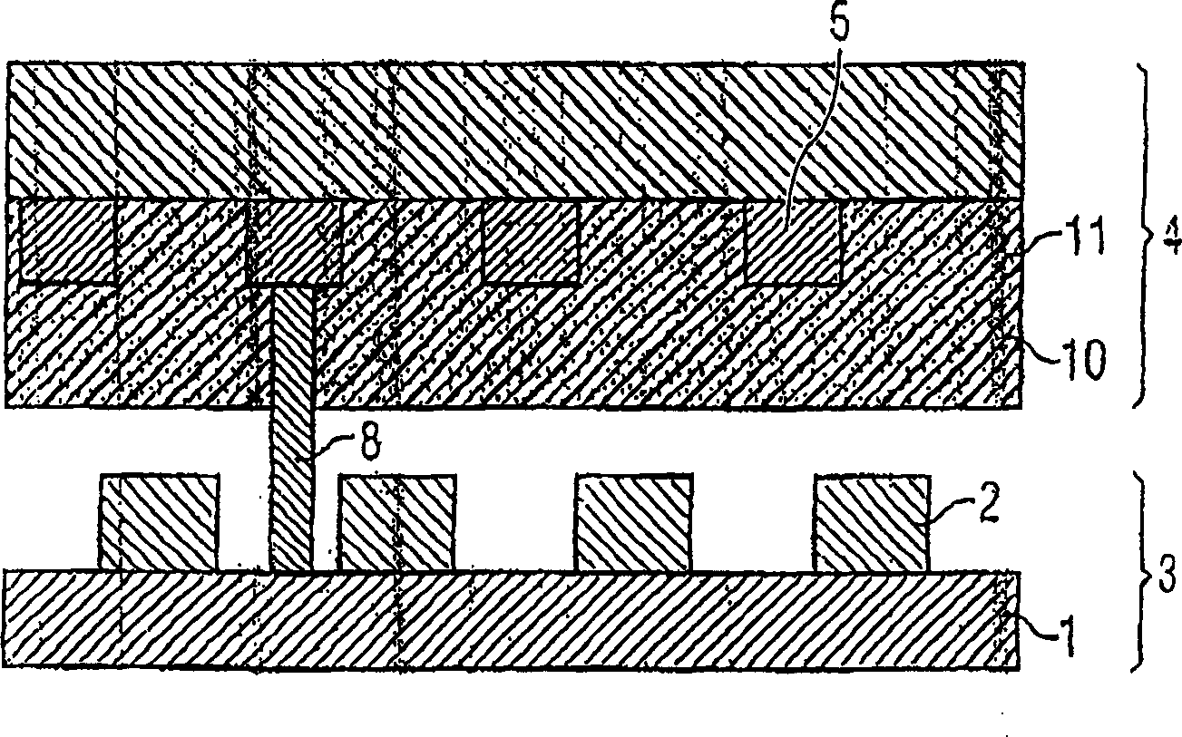
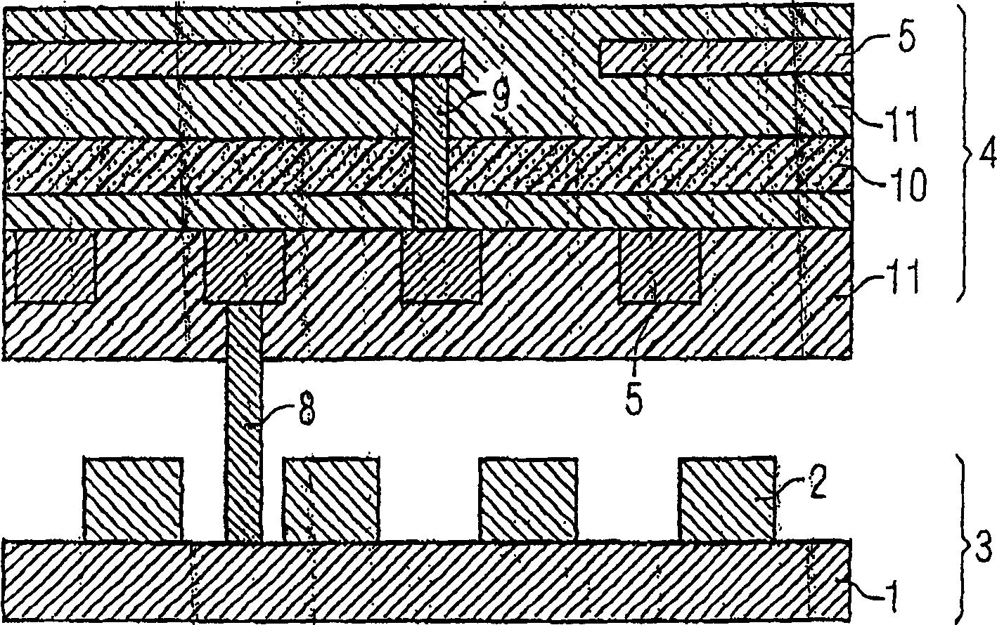
[0026] Figure 1 shows a semiconductor device consisting of an active region (3) and a metallization layer (4). The active area (3) is divided into two parts, the bit line (1) and the word line (2). The metallization layer (4) has at least one metal plane (5) and an intermetallic dielectric (11), if there are several metal planes (5), these metal planes (5) are stacked together in a layered manner and are The intermetallic dielectric (11) in between is electrically insulated.

[0027] Between the bit line (1) and the metal plane (5) there is a connecting line (8), the so-called "Vias". In the manufacturing process, the semiconductor device is constructed from the bottom to the top starting from the active area (3). Therefore, after the construction of the active region (3) is completed, a heating step is performed to eliminate and / or remove the carriers fixed by the ultraviolet rays from the memory layer.

[0028] Since the semiconductor device will be exposed to high-energy...


PUM


Abstract

A semiconductor configuration has an active region, a metalization layer having at least one metal plane, and connecting lines between the active region and the metalization layer. The least one metal plane is embedded in an intermetal dielectric. A UV protection plane is integrated with the metalization layer. A method for fabricating such a semiconductor configuration is also provided.

Description

technical field [0001] The present invention relates to a semiconductor device. This semiconductor device has an active area and a metallization layer. The metallization layer is at least composed of a first metal plane and a connection line between the active area and the metallization layer. At least one metal plane of the metallization layer is buried within an intermetal dielectric. Background technique [0002] During the manufacturing process of semiconductor devices, ultraviolet light is used to expose the structure of metal planes. In addition, plasmas that emit ultraviolet light are generated during the formation of other coatings. Ultraviolet light can cause defects in the crystal structure of semiconductor materials, resulting in adverse effects on the functions of semiconductor devices. This UV-induced defect can be repaired by a heat treatment procedure at a temperature of about 450°C. [0003] However, it is not suitable to use heat treatment to repair the c...

Claims


Application Information

Patent Timeline
Patent Type & Authority Applications(China)
IPC IPC(8): H01L21/8246H01L23/552H01L27/115
CPCH01L2924/0002H01L23/552H01L27/115H01L27/11568H10B69/00H10B43/30H01L2924/00
Inventor M·沃格特V·波尔伊S·里伊德尔E·S·冯卡米恩斯基
Owner INFINEON TECH AG
Why Eureka
Try Eureka