A display panel, its manufacturing method and display device

A technology for a display panel and a manufacturing method, applied in the field of display panels and display devices, capable of solving problems such as viewing angle deviation, brightness and chromaticity differences, and achieving the effect of improving viewing angle deviation

Active Publication Date: 2022-05-27
BOE TECH GRP CO LTD
View PDF8 Cites 0 Cited by
  • Summary
  • Abstract
  • Description
  • Claims
  • Application Information

AI Technical Summary

Problems solved by technology

[0003] However, in the top-emitting organic electroluminescent device structure, the metal cathode and the reflective metal at the bottom form a resonant cavity (microcavity structure), and the light of the wavelength satisfying the resonance condition will be strengthened due to constructive interference. , the distance between the light passing through the metal cathode and the reflective metal at the bottom will change accordingly, that is to say, the paths of light passing through different viewing angles are different, resulting in differences in brightness and chromaticity under different viewing angles
Therefore, the current top-emitting organic electroluminescent devices have a serious problem of angular misalignment.

Method used


Image

  • A display panel, its manufacturing method and display device
  • A display panel, its manufacturing method and display device
  • A display panel, its manufacturing method and display device

Examples


Embodiment Construction

[0033] Aiming at the problem of serious viewing angle deviation in the top-emitting organic electroluminescent device in the prior art, the embodiments of the present invention provide a display panel, a manufacturing method thereof, and a display device.

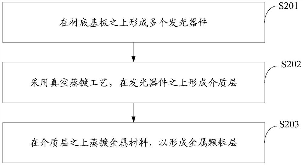
[0034] The specific implementations of the display panel, the manufacturing method thereof, and the display device provided by the embodiments of the present invention will be described in detail below with reference to the accompanying drawings. The thickness and shape of each film layer in the drawings do not reflect the actual scale, and are only intended to illustrate the content of the present invention.

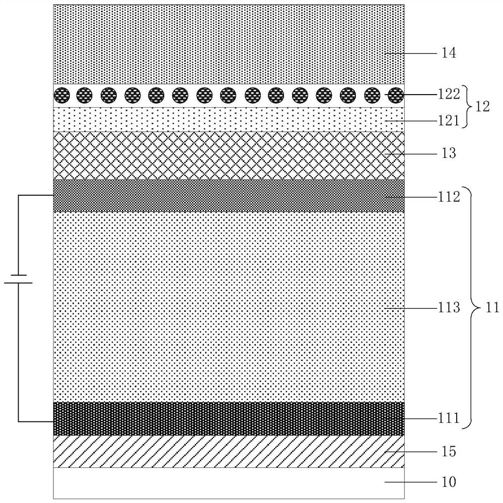
[0035] In a first aspect, an implementation of the present invention provides a display panel, such as figure 1 shown, including:

[0036] base substrate 10;

[0037] a plurality of light emitting devices 11 located on the base substrate 10;

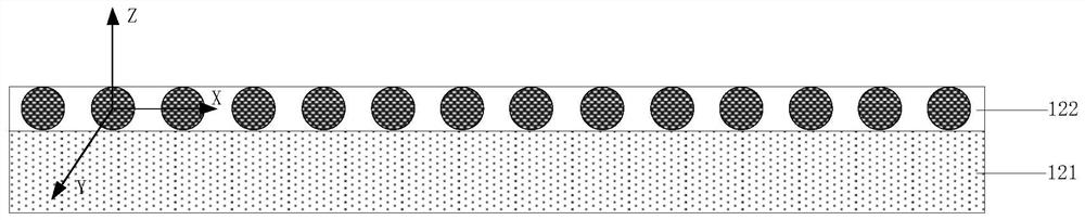
[0038] The light scattering layer 12 is located on one side of the ligh...


PUM

PropertyMeasurementUnit
thicknessaaaaaaaaaa
thicknessaaaaaaaaaa

Abstract

The invention discloses a display panel, a manufacturing method thereof and a display device. The display panel comprises: a base substrate; a plurality of light-emitting devices located on the base substrate; a light scattering layer located on the light-emitting surface side of the light-emitting devices The light scattering layer includes: a dielectric layer located on the side of the light-emitting device away from the substrate, and a metal particle layer located on the side of the dielectric layer away from the light-emitting device. In the above-mentioned display panel provided by the embodiment of the present invention, by providing a light scattering layer on the light-emitting surface side of the light-emitting device, the metal particle layer in the light-scattering layer has a light-scattering effect, which can change the direction of the light emitted by the light-emitting device and play a role The problem of viewing angle deviation is improved, and since the metal particle layer is located on the side of the light-emitting surface of the light-emitting device, it will not affect the electrical characteristics of the light-emitting device.

Description

technical field [0001] The present invention relates to the field of display technology, and in particular, to a display panel, a manufacturing method thereof and a display device. Background technique [0002] Organic electroluminescent devices (Organic Light-Emitting Diode, OLED) have attracted great attention in the field of flat panel display and lighting due to their advantages of high brightness, color saturation, thinness and flexibility. At present, the structures of common organic electroluminescent devices include top light emitting device structure and bottom light emitting device structure. Compared with the bottom light emitting device structure, the top light emitting device structure has the advantages of high aperture ratio, high color purity, and easy realization of high pixels. Density (Pixels Per Inch, PPI) and other advantages, it has become the current mainstream organic electroluminescent device structure. [0003] However, in the structure of the top-...

Claims


Application Information

Patent Timeline
Patent Type & Authority Patents(China)
IPC IPC(8): H01L51/52H01L51/56
CPCH10K50/85H10K71/00
Inventor 李彦松吴海东暴营樊星杜小波
Owner BOE TECH GRP CO LTD
Why Eureka
Try Eureka