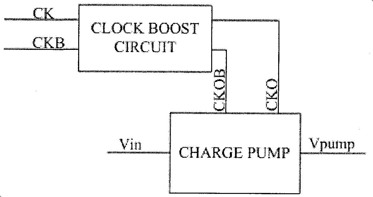
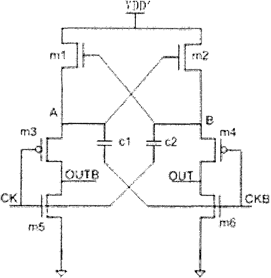
Boosting clock circuit and charge pump provided with the same
A clock circuit, charge pump technology, applied in the field of charge pump, to overcome the discharge current, the effect of accumulating charge stability
- Summary
- Abstract
- Description
- Claims
- Application Information
AI Technical Summary
Problems solved by technology
Method used
Image
Examples
Embodiment Construction
[0044] In order to make the object, technical solution and advantages of the present invention clearer, the present invention will be further described in detail below in conjunction with the accompanying drawings.
[0045] Such as figure 2 As shown, from the point of view of charging the capacitor, the capacitance of each single-stage boost clock circuit is set to C, and the charging voltage is VDD', then the charging charge of the single-stage boost clock circuit Q=C*VDD'. N stages of single-stage boosted clock circuits are connected in series; the capacitance of each stage of single-stage boosted clock circuit can be different, which are C1~CN respectively; the power supply voltage of each stage of single-stage boosted clock circuit can also be different, respectively: VDD 1~VDD N (such as image 3 shown). Then the charge Q' accumulated by the entire boost clock circuit = Q1+Q2+...+QN=C1*VDD 1+C2*VDD 2+...+CN*VDD N. To reduce the adverse effects caused by too much charg...
PUM
 Abstract
Description
Claims
Application Information


