Boosting clock circuit and charge pump with same

A technology of clock circuit and charge pump, which is applied in the field of charge pump, can solve problems such as temperature and humidity, and achieve the effect of overcoming large errors and stabilizing the difference between high and low levels

Active Publication Date: 2012-03-21
SHANGHAI HUAHONG GRACE SEMICON MFG CORP
View PDF4 Cites 0 Cited by
  • Summary
  • Abstract
  • Description
  • Claims
  • Application Information

AI Technical Summary

Problems solved by technology

[0010] However, in actual circuits, the boost clock circuit has factors that change its boost characteristics, such as various parasitic capacitances, environmental factors such as temperature and humidity
Direct detection of the power supply voltage VDD' or the change of the input voltage VIN that has a fixed corresponding relationship with the power supply voltage VDD' cannot completely and directly reflect the voltage change of the actual boost clock circuit, because the actual circuit is not considered at this time. Various parasitic capacitances, environmental factors such as temperature and humidity
Therefore, directly detecting the change result of the supply voltage VDD' or the input voltage VIN that has a fixed corresponding relationship with the supply voltage VDD' to select the size of the charging capacitor of each single-stage boost clock circuit has a large error in actual circuit applications.

Method used


Image

  • Boosting clock circuit and charge pump with same
  • Boosting clock circuit and charge pump with same
  • Boosting clock circuit and charge pump with same

Examples


Embodiment Construction

[0048] In order to make the object, technical solution and advantages of the present invention clearer, the present invention will be further described in detail below in conjunction with the accompanying drawings.

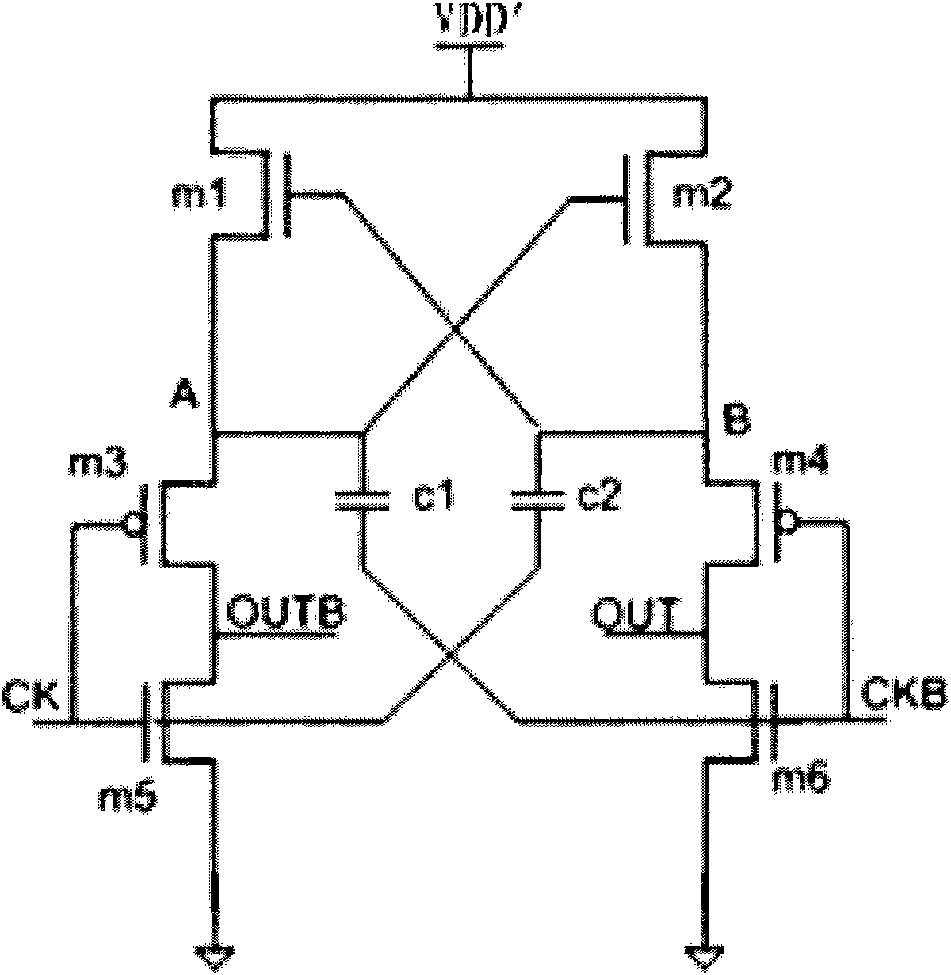
[0049] Figure 4 It is a schematic structural diagram of a single-stage boost clock circuit adopted in the boost clock circuit provided by the present invention. Compare Figure 4 and figure 2 It can be seen from the figure that the difference between the single-stage boosted clock circuit of this embodiment and the traditional single-stage boosted clock circuit is that the capacitance thereof is adjustable. The capacitor of the single-stage boost clock circuit is a variable capacitor C'100. The size of the variable capacitor C'100 is adjusted by the comparison and selection circuit connected to it according to the variation of its own input voltage. Specifically, the variable capacitor C'100 may be composed of one or more capacitors connected in parallel, an...


PUM


Abstract

A boosting clock circuit comprises N stages of single-stage boosting clock circuits (CK_BST 1-CK_BST N) in a cascading connection manner, wherein at least one stage of single-stage boosting clock circuit is connected with a comparison selection circuit, the power supply voltage VDD' of all single-stage boosting clock circuits is the same, and the boosting clock circuit is characterized in that the at least one comparison selection circuit is connected with a tracking circuit; the input voltage VIN of the tracking circuit and the power supply voltage VDD' of the ingle-stage boosting clock circuit meet the following relation: VIN=F (VDD'), wherein N is an integral number larger than or equal to 1, and F is a fixed function. A charge pump circuit comprises a charge pump and the boosting clock circuit with the tracking circuit and the comparison selection circuit, wherein the boosting clock circuit charges the charge pump. The boosting clock circuit and the charge pump circuit overcome the problems that the traditional boosting clock circuit with the comparison selection circuit, and the charge pump circuit have large errors in the practical application, and can better meet the requirement of practical application.

Description

technical field [0001] The invention belongs to the technical field of charge pumps, in particular to a boost clock circuit and a charge pump with the boost clock circuit. Background technique [0002] A charge pump, also known as a switched capacitor voltage converter, is a DC-DC (DC-DC) converter that uses "flying" or "pumping" capacitors to store energy. The charge pump can make the input voltage Raised or lowered, can also be used to generate negative voltages. Traditional charge pumps control the charging and discharging of flying capacitors to multiply or reduce the input voltage by a certain factor (0.5, 2 or 3) to obtain the required output voltage. [0003] At present, commonly used charge pumps have a boost clock circuit. The input clock signal CK and the reverse clock signal CKB are boosted by the boost clock circuit and output as the clock signal CKO and the reverse clock signal CKOB; the corresponding high-low level difference VH of the clock signal CK and the...

Claims


Application Information

Patent Timeline
Patent Type & Authority Applications(China)
IPC IPC(8): H02M3/07
Inventor 杨光军
Owner SHANGHAI HUAHONG GRACE SEMICON MFG CORP
Why Eureka
Try Eureka