Liquid crystal display, liquid crystal display driving method, and television receiver

A liquid crystal display device, potential technology, applied in TV, TV system components, electrical components, etc., can solve problems such as difficult pixel charging, increased resistance of data signal line wiring, etc.

Inactive Publication Date: 2010-12-01
SHARP KK
View PDF1 Cites 28 Cited by
  • Summary
  • Abstract
  • Description
  • Claims
  • Application Information

AI Technical Summary

Problems solved by technology

[0002] Liquid crystal display devices are becoming larger and more high-definition, but the number of pixels is also increasing, and the wiring resistance of data signal lines is also increasing, making it difficult to fully charge each pixel.

Method used


Image

  • Liquid crystal display, liquid crystal display driving method, and television receiver
  • Liquid crystal display, liquid crystal display driving method, and television receiver
  • Liquid crystal display, liquid crystal display driving method, and television receiver

Examples


Embodiment approach 1

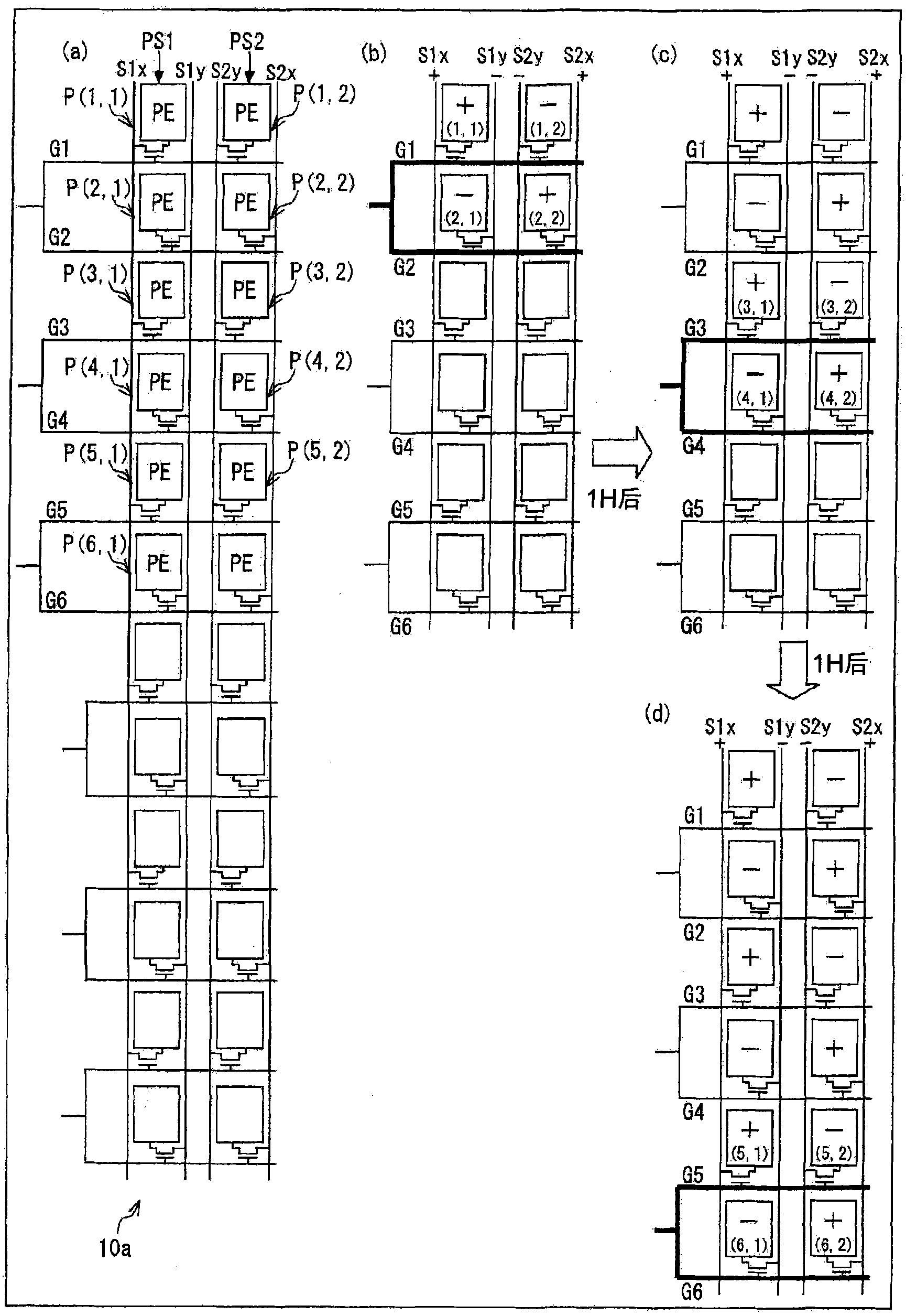
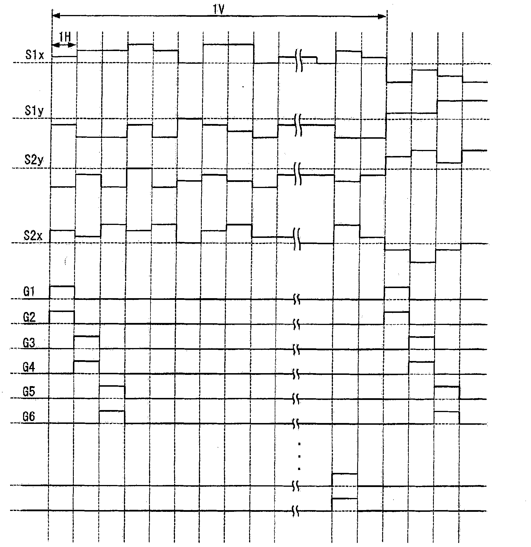
[0115] figure 1 (a) is a schematic diagram showing a configuration example of a display portion of the present liquid crystal display device, figure 1 (b) to (d) are schematic diagrams showing a driving method of the display unit, figure 2 is a timing chart showing this driving method. Such as figure 1 As shown in (a), in the display portion 10a, first and second data signal lines (for example, S1x and S1y) are provided corresponding to one pixel row (for example, PS1), and one pixel (for example, PS1) included in the pixel row P(1,1)) is connected to one scan signal line (for example, G1), and is connected to one of the first and second data signal lines (for example, S1x and S1y). Specifically, starting from the first row of pixels in each pixel column, two pixels adjacent in the column direction are regarded as a pair in sequence, and when considered sequentially in this order, the two pixels of each pair have different data The signal lines are connected, and for two ...

Embodiment approach 2

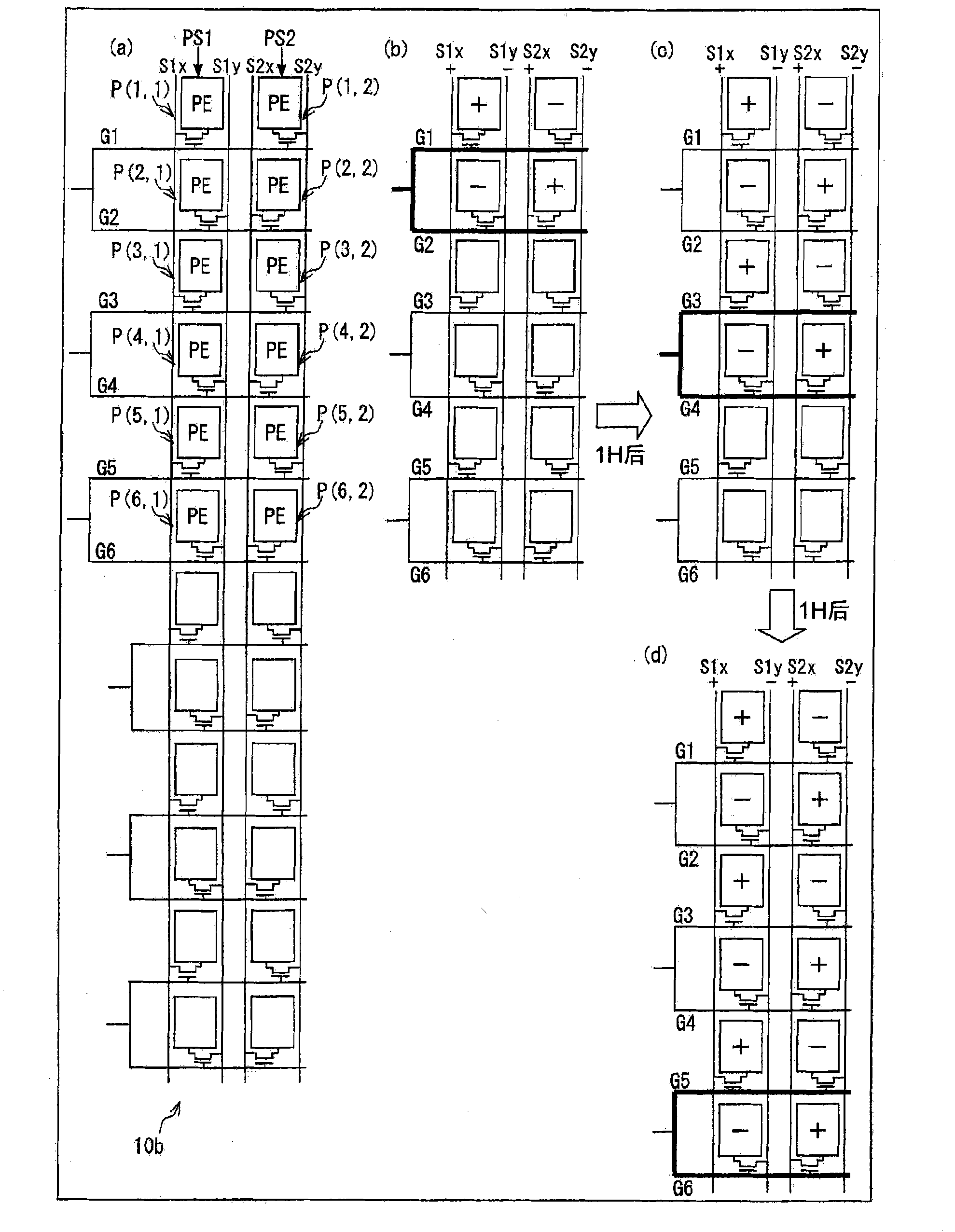
[0143] Figure 13 (a) is a schematic diagram showing a configuration example of a display portion of the present liquid crystal display device, Figure 13 (b) to (d) are schematic diagrams showing a driving method of the display unit, Figure 14 is a timing chart showing this driving method. Such as Figure 13 As shown in (a), in the display portion 10e, first and second data signal lines (for example, S1x and S1y) are provided corresponding to one pixel column (for example, PS1), and one pixel ( For example, P(1, 1)) is connected to one scan signal line (for example, G1) and connected to one of the first and second data signal lines (for example, S1x and S1y). Specifically, starting from the pixel in the first row of each pixel column, two pixels adjacent in the column direction are regarded as a pair in sequence, and when considered sequentially in this order, the two pixels of each pair and different data signals For two consecutive pairs, the data signal lines connecte...

Embodiment approach 3

[0171] Figure 25 (a) is a schematic diagram showing a configuration example of a display portion of the present liquid crystal display device, Figure 25 (b) to (d) are schematic diagrams showing a driving method of the display unit, Figure 26 is a timing chart showing this driving method. Such as Figure 25As shown in (a), in the display portion 10i, first and second data signal lines (for example, S1x and S1y) are provided corresponding to one pixel row (for example, PS1), and one pixel (for example, PS1) included in the pixel row , P(1, 1)) is connected to one scan signal line (for example, G1) and connected to one of the first and second data signal lines (for example, S1x and S1y). Specifically, starting from the first row of pixels in each pixel column, two adjacent pixels in the column direction are sequentially regarded as a pair, and two adjacent pairs are sequentially regarded as a group, and when considered sequentially in this order , in each group, each pair...


PUM


Abstract

First and second data signal lines (for example, S1x, S1y) are provided for a column of pixels (for example, PS1), and signal potentials of opposite polarity to each other are supplied to the data signal lines respectively. A predetermined pixel (P(1, 1)) is taken as the first pixel. A pixel (for example, P(2, 1) for n=i=1) other than the (2xnxi+1)-th pixel in the scanning direction is connected to a data signal line (for example, S1y) different from that connected to the previous pixel, whereas the (2xnxi+1)-th pixel (for example, P(3, 1) for n=i=1) is connected to the same data signal line (for example, S1y) as that connected to the previous pixel. The polarity of the signal potential supplied to each data signal line is inverted every n horizontal scanning periods (for example, 1H). Every adjacent two scan signal lines starting from the scan signal line (G1) connected to the predetermined pixel are sequentially selected at the same time among scan signal lines (G1, G2,...). A liquid crystal display with this structure enables an increase of the pixel charging time as well as prevention of flickering.

Description

technical field [0001] The present invention relates to a liquid crystal display device that simultaneously performs writing to a plurality of pixels included in the same pixel column. Background technique [0002] Liquid crystal display devices are increasing in size and definition, but the number of pixels is also increasing, and the wiring resistance of data signal lines is also increasing, making it difficult to sufficiently charge each pixel. Here, Patent Document 1 discloses a structure in which two data signal lines are provided for one pixel column, and scanning signal lines respectively connected to adjacent two pixels are selected at the same time. In addition, the polarity of the signal potential supplied to each data signal line is inverted every frame. With this structure, it is possible to simultaneously write signal potentials to two pixels, so that the charging time of each pixel can be increased. [0003] Patent Document 1: Japanese Laid-Open Patent Public...

Claims


Application Information

Patent Timeline
Patent Type & Authority Applications(China)
IPC IPC(8): G09G3/36G02F1/133G09G3/20
CPCG09G2320/0247G02F1/136286G09G2300/0447G09G3/3614H04N5/00G09G2300/0426G09G3/3648G09G3/3688G09G2320/028G09G3/3607G09G3/3677G09G2310/0289G09G2310/021G09G3/2096G09G3/3666G02F2203/30
Inventor 杉原利典伴厚志津幡俊英
Owner SHARP KK
Why Eureka
Try Eureka