Method for manufacturing a microelectronic package comprising at least one microelectronic device

A technology of microelectronic packaging and microelectronic devices, applied in the direction of electric solid state devices, electrical components, semiconductor devices, etc., to achieve the effect of increasing cost price, reducing cost price, and cheap manufacturing process

Inactive Publication Date: 2011-11-23
NXP BV
View PDF0 Cites 0 Cited by
  • Summary
  • Abstract
  • Description
  • Claims
  • Application Information

AI Technical Summary

Problems solved by technology

In practice, about ten times the sheet surface required to form the leadframe is discarded when making leadframes using this method

Method used


Image

  • Method for manufacturing a microelectronic package comprising at least one microelectronic device
  • Method for manufacturing a microelectronic package comprising at least one microelectronic device

Examples


Embodiment Construction

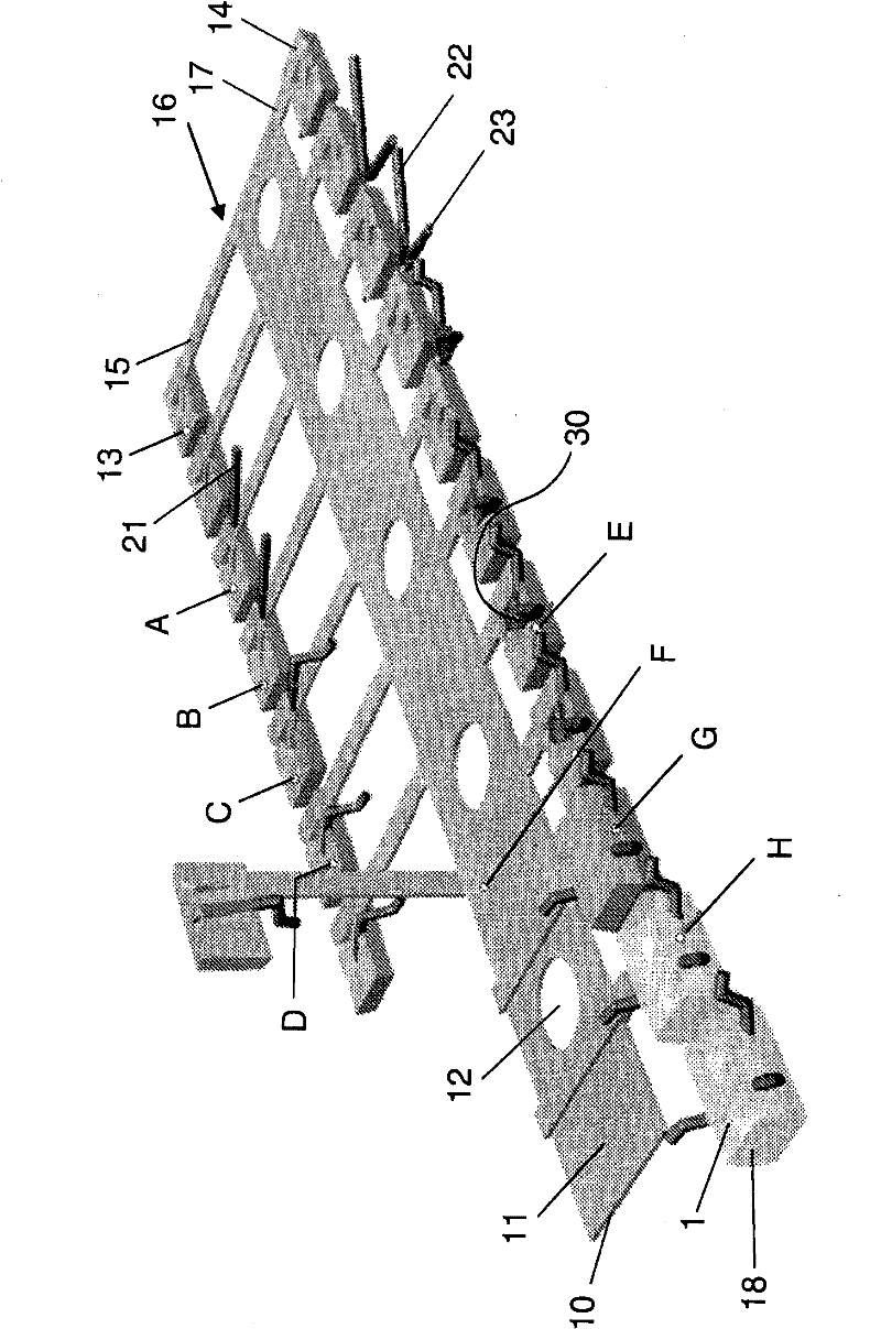
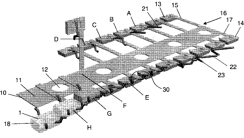
[0038] figure 1 Successive steps of a process for manufacturing a microelectronic package 1 according to the invention are shown.

[0039] At the beginning of the manufacturing process of the microelectronic package 1, a carrier 10 is provided. Preferably, the carrier 10 comprises plastic, the carrier 10 being manufactured by applying injection molding techniques. In the example shown, the carrier 10 comprises an elongated central strip 11 having a pattern of holes 12 . Furthermore, the carrier 10 comprises a pair of encapsulation components 13 , 14 , wherein each encapsulation component 13 , 14 of the pair of encapsulation components 13 , 14 is arranged on the other side of the central strip 11 . One of the packaged components 13, 14 of each packaged component 13, 14 pair is connected to the central strip 11 by an elongated, relatively thin connecting member 15, wherein the entirety of the connecting member 15 and the packaged component 13 is rotatably connected to the cent...


PUM


Abstract

A method for manufacturing a microelectronic package (1) comprises the steps of providing two parts (13, 14) comprising electrically insulating material such as plastic; providing members (21, 22, 23) comprising electrically conductive material; providing a microelectronic device (30); positioning the electrically conductive members (21, 22, 23) and the microelectronic device (30) on the electrically insulating parts (13, 14); and placing the electrically insulating parts (13, 14) against each other, wherein the microelectronic device (30) and portions of the electrically conductive members (21, 22, 23) are sandwiched between the electrically insulating parts (13, 14). The electrically conductive members (21, 22, 23) are intended to be used for realizing contact of the microelectronic device (30) arranged inside the package (1) to the external world. An important advantage of the method having steps as mentioned is that the electrically conductive members (21, 22, 23) as such are provided, wherein it is not necessary to provide a conventional lead frame which has the disadvantage of causing considerable waste of metal material during its manufacturing process.

Description

technical field [0001] The present invention relates to methods of fabricating microelectronic packages including at least one microelectronic device (eg, processor chip, transistor, sensor die, diode, light emitting diode (LED), etc.), and to microelectronic packages. Background technique [0002] Microelectronic packages in which at least one microelectronic device is arranged are well known and various types of such packages have been developed. Among other things, encapsulation is used to protect the microelectronic device and to allow the microelectronic device to be easily connected to another device. Typically, microelectronic device dimensions are in the micrometer range and packages are in the millimeter range. [0003] Typically, in order to support the microelectronic devices and to ensure the required robustness of the microelectronic package, a carrier substrate is provided to which the microelectronic devices are attached. In a typical embodiment of a microel...

Claims


Application Information

Patent Timeline
Patent Type & Authority Patents(China)
IPC IPC(8): H01L21/56
CPCH01L24/97H01L21/56H01L2924/01029H01L2924/12041H01L24/13H01L24/16H01L24/81H01L2224/13101H01L2224/13144H01L2224/16245H01L2224/81203H01L2224/81805H01L2924/00015H01L2924/01322H01L2924/15747H01L2224/85H01L2924/014H01L2924/00014H01L2924/00
Inventor 保卢斯·M·C·海森安东尼厄斯·J·G·M·范登伯克里查德·范利斯豪特
Owner NXP BV
Why Eureka
Try Eureka