Cutting method of semiconductor wafer

A cutting method and semiconductor technology, applied in the fields of semiconductor devices, semiconductor/solid-state device manufacturing, electrical components, etc., can solve the problems of increased cost, cost increase, slow laser cutting speed, etc., and achieve the effect of improving production speed and reducing cost.

Inactive Publication Date: 2010-12-29
AUSK OPTOELECTRONICS
View PDF0 Cites 22 Cited by
  • Summary
  • Abstract
  • Description
  • Claims
  • Application Information

AI Technical Summary

Problems solved by technology

[0004] However, in the laser cutting process, because the laser cutting speed is extremely slow, in order to meet the requirements of mass production, many laser cutting machines need to operate at the same time, which greatly increases the cost; especially when the size of the die is smaller or the substrate is thinner. When large, the required cost doubles

Method used


Image

  • Cutting method of semiconductor wafer
  • Cutting method of semiconductor wafer
  • Cutting method of semiconductor wafer

Examples


Embodiment Construction

[0039] A method for dicing a semiconductor wafer according to a preferred embodiment of the present invention will be described below with reference to related drawings.

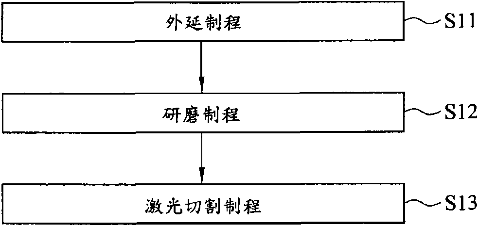
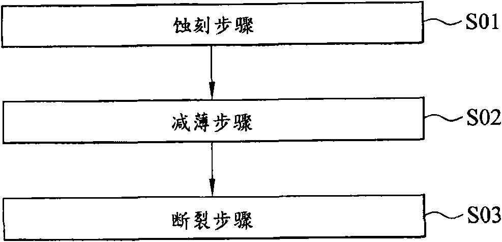
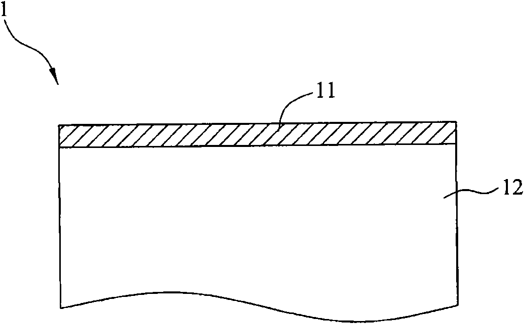
[0040] Please refer to figure 2 As shown, a method for cutting a semiconductor wafer according to a preferred embodiment of the present invention includes steps S01 to S03. Please refer to the semiconductor wafer 1 of the present embodiment Figure 3A As shown, the semiconductor wafer 1 has an active layer 11 and a substrate 12 . Wherein, the active layer 11 may include semiconductor circuits with any functions, and is not limited here, such as functions such as light emission, calculation, switching, sensing, and power generation. In addition, the present invention does not limit the material and shape of the substrate 12 , and the material of the substrate 12 may include, for example, glass, ceramics, metal, plastic, resin, or sapphire. In this embodiment, the semiconductor wafer 1 is an example of a l...


PUM


Abstract

The invention discloses a cutting method of a semiconductor wafer. The wafer comprises an active layer and a base plate. The cutting method comprises the step of etching the active layer to form at least one groove, thinning a base plate and fracturing the wafer at the groove by external force or stress. In the invention, the groove is formed by etching the active layer without using a laser cutting technique, and the wafer is fractured at the groove by the fracturing step to form a plurality of tube cores, so that the cost is deceased.

Description

technical field [0001] The invention relates to a cutting method, in particular to a semiconductor wafer cutting method. Background technique [0002] A light emitting diode (LED) is a light emitting element made of semiconductor materials. Since the light-emitting diode device is cold light-emitting, it has the advantages of low power consumption, long component life, fast response speed, etc. Progress, its application scope covers the indicator lights of computers or home appliances, the backlight of liquid crystal display devices, and even traffic signs or vehicle lights. [0003] Generally speaking, three-stage processes are required to produce LED dies for application in back-end products. Such as figure 1 As shown, the three-stage process includes step S11 to step S13 in sequence, wherein step S11 is an epitaxial process, step S12 is a grinding process, and step S13 is a laser cutting process. An N-type semiconductor layer, a light-emitting layer and a P-type semic...

Claims


Application Information

Patent Timeline
Patent Type & Authority Applications(China)
IPC IPC(8): H01L21/78H01L33/00H01L21/302H01L21/304
Inventor 林崇智
Owner AUSK OPTOELECTRONICS
Why Eureka
Try Eureka