Charge transfer circuit suitable for common CMOS process and charge transfer control switch thereof

A charge transmission and control switch technology, applied in the direction of analog-to-digital converters, etc., can solve the problems of limiting speed and precision, and achieve the effect of precise charge addition and subtraction operations

Active Publication Date: 2013-07-03
58TH RES INST OF CETC
View PDF3 Cites 0 Cited by
  • Summary
  • Abstract
  • Description
  • Claims
  • Application Information

AI Technical Summary

Problems solved by technology

The use of these high-gain and wide-bandwidth operational amplifiers limits the speed and accuracy of switched-capacitor pipelined ADCs, and becomes the main bottleneck limiting the performance improvement of this type of ADC. The level of consumption increases linearly with the increase of speed

Method used


Image

  • Charge transfer circuit suitable for common CMOS process and charge transfer control switch thereof
  • Charge transfer circuit suitable for common CMOS process and charge transfer control switch thereof
  • Charge transfer circuit suitable for common CMOS process and charge transfer control switch thereof

Examples


Embodiment Construction

[0040] The preferred embodiments of the present invention will be described in detail below with reference to the accompanying drawings.

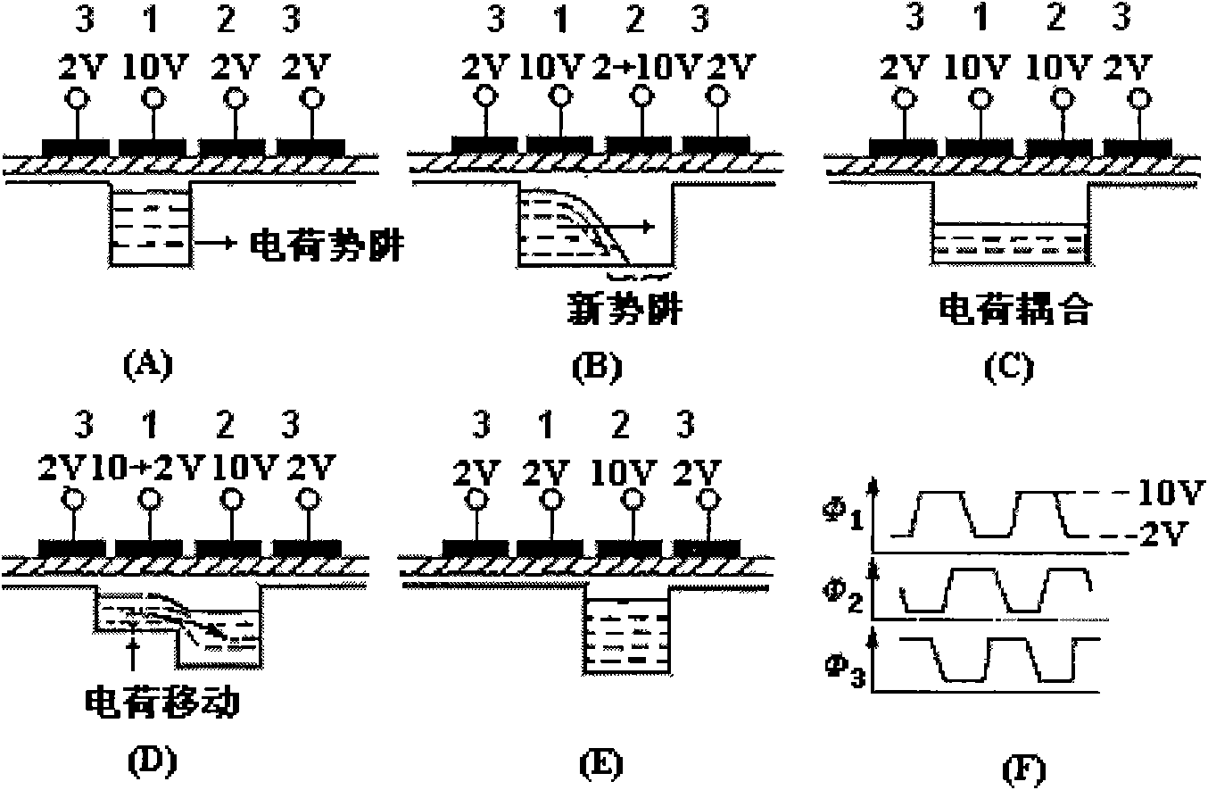
[0041] figure 1 Shown is a schematic diagram of the charge transport principle of the CCD device. The charge transfer process refers to the transfer of charges in the CCD potential well from one location to another. exist figure 1 In (A), it is assumed that a charge packet has been stored in the potential well under the second electrode, the voltage on this electrode is 10V, and the voltage on the other three electrodes is 2V (2V>Vth), then there are potentials under all electrodes Well, it's just that the potential well under the 10V electrode is much deeper than the potential well under the 2V electrode. figure 1 In (B), if the voltage under the third electrode is increased to 10V, the potential wells under the second and third electrodes will merge, and the charge packets under the second electrode will be distributed among the two po...


PUM


Abstract

The invention provides a high-precision charge addition-subtraction transfer circuit suitable for a common CMOS process and a charge transfer control switch thereof. The charge addition-subtraction transfer circuit comprises a charge transfer switch, a first charge storage node, a first charge storage capacitor, a second charge storage node, a second charge storage capacitor and a third storage capacitor, wherein the first charge storage capacitor is connected to the first charge storage node, and the second charge storage capacitor and the third charge storage capacitor are connected to the second charge storage node. The charge addition-subtraction transfer circuit can realize accurate charge addition-subtraction operation and accurately control the quantity of transferred charge, and can be widely used in charge coupled secondary flowing water circuit at all levels in a charge coupled pipeline AD converter.

Description

technical field [0001] The invention relates to a high-precision charge addition and subtraction transmission circuit suitable for common CMOS technology and a charge transmission control switch thereof. Background technique [0002] With the continuous development of digital signal processing technology, the digitization and integration of electronic systems is an inevitable trend. However, most signals in reality are continuously changing analog quantities, which need to be transformed into digital signals through analog-to-digital conversion before they can be input into digital systems for processing and control. Therefore, analog-to-digital converters are indispensable in future digital system design. Part. In applications such as broadband communications, digital high-definition television, and radar, systems require analog-to-digital converters with both very high sampling rates and resolutions. Portable terminal products in these application fields require not only...

Claims


Application Information

Patent Timeline
Patent Type & Authority Patents(China)
IPC IPC(8): H03M1/12
Inventor 陈珍海季惠才黄嵩人吴俊于宗光
Owner 58TH RES INST OF CETC
Why Eureka
Try Eureka