Supercharge Your Innovation With Domain-Expert AI Agents!

Interfacing between differing voltage level requirements in an integrated circuit system

An integrated circuit, power supply voltage technology, applied in the direction of logic circuit connection/interface layout, logic circuit coupling/interface using field effect transistors, fail-safe circuits, etc., can solve problems such as gate (G) oxide damage

Inactive Publication Date: 2011-05-11
AVAGO TECH WIRELESS IP SINGAPORE PTE
View PDF3 Cites 1 Cited by
  • Summary
  • Abstract
  • Description
  • Claims
  • Application Information

AI Technical Summary

Problems solved by technology

[0004] Considering a MOS transistor as an active element, when the voltage between the drain (D) terminal and gate (G) terminal of the MOS transistor exceeds the upper limit value, the gate (G) oxide of the stressed MOS transistor will damage

Method used


Image

  • Interfacing between differing voltage level requirements in an integrated circuit system
  • Interfacing between differing voltage level requirements in an integrated circuit system
  • Interfacing between differing voltage level requirements in an integrated circuit system

Examples


Embodiment Construction

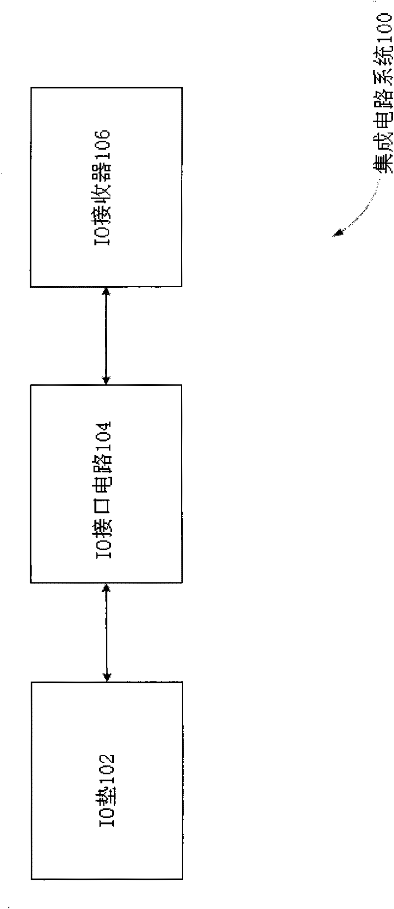
[0024] The exemplary embodiments described below may be used to implement input / output (IO) interface circuits capable of interfacing between different voltage level requirements. Although these embodiments have been described with reference to specific exemplary embodiments, it will be evident that various modifications and changes may be made to these embodiments without departing from the broad spirit and scope of the various embodiments.

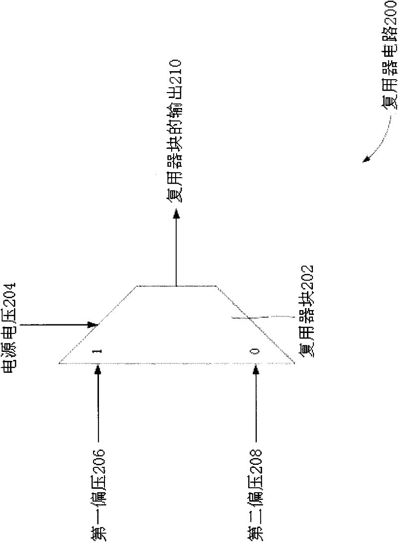
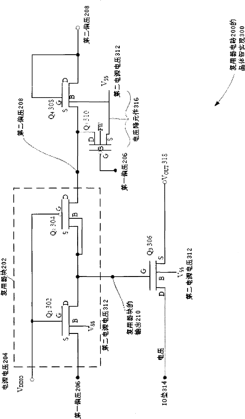
[0025] figure 2 A multiplexer circuit 200 is shown in accordance with one or more embodiments. In one or more embodiments, the multiplexer circuit 200 includes a multiplexer block 202 that can receive as inputs a first bias voltage 206 and a second bias voltage 208 . In one or more embodiments, the first bias voltage 206 can be controllably generated from a supply voltage 204 and the second bias voltage 208 can be controllably generated from an external voltage provided through an input / output (IO) pad. In one or more embodiments, the...


PUM


Abstract

A method includes controllably generating a first bias voltage from a supply voltage to be within an upper tolerable limit of an operating voltage of an IO receiver, and controllably generating a second bias voltage from an external voltage supplied through an IO pad to be within the upper tolerable limit of the operating voltage of the IO receiver. The method also includes deriving an output voltage from the first bias voltage during a normal condition and a tolerant condition, and deriving the output voltage from the second bias voltage during a failsafe condition. The tolerant condition isa mode of operation where the external voltage supplied through the IO pad varies from zero to a value higher than the supply voltage, and the failsafe condition is a mode of operation where the supply voltage is zero.

Description

technical field [0001] The present disclosure relates generally to electronic circuits and, more particularly, to systems, apparatus and methods for implementing input / output (IO) interface circuits capable of reliably interfacing between different voltage level requirements. Background technique [0002] Such as figure 1 As shown, an input / output (IO) interface circuit 104 may interface an IO pad 102 of an integrated circuit (IC) with an IO receiver 106 . IO pads can allow the IC to connect to external devices. figure 1 IC system 100 may require different voltage levels for IO pad 102 and IO receiver 106 . For example, the voltage at the IO pad 102 may be high (eg, 3.465, 5.5V, or 3.3V+5% tolerance, 5V+10% tolerance) while the operating voltage of the IO receiver may be low (eg, 2.5V). The supply voltages may also be at different voltage levels. [0003] The constituent active components of the IO interface circuit 104 and the IO receiver 106 (for example, metal-oxide-s...

Claims


Application Information

Patent Timeline
IPC IPC(8): H03K19/007H03K19/0185
CPCH03K17/693H03K19/00315H03K19/007H03K19/0175
Inventor 潘卡吉·库马尔普拉姆德·E·帕拉梅斯沃兰梅卡什沃·克桑德拉曼维尼·德什潘德约翰·克瑞兹
Owner AVAGO TECH WIRELESS IP SINGAPORE PTE
Features
  • R&D
  • Intellectual Property
  • Life Sciences
  • Materials
  • Tech Scout
  • Unparalleled Data Quality
  • Higher Quality Content
  • 60% Fewer Hallucinations
Learn More