Liquid crystal display device
A technology of liquid crystal display device and liquid crystal display panel, which is applied to lighting devices, fixed lighting devices, components of lighting devices, etc., can solve the problems of increasing the burden on the earth's environment, and achieve the effect of small size
- Summary
- Abstract
- Description
- Claims
- Application Information
AI Technical Summary
Problems solved by technology
Method used
Image
Examples
Embodiment 1
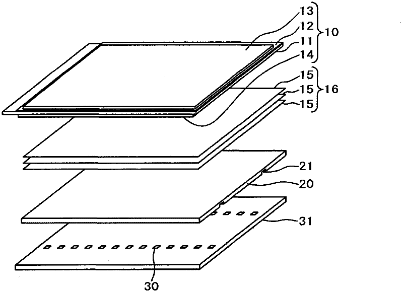
[0067] figure 1 It is an exploded perspective view of a liquid crystal display device. figure 1 Divided into a liquid crystal display panel 10 and a backlight source. exist figure 1 Among them, the TFT substrate 11 on which the display area, scanning lines, image signal lines, etc., in which TFTs and pixel electrodes are arranged in a matrix, is formed, and the counter substrate 12 on which color filters, etc. are formed are bonded by an adhesive (not shown). . Liquid crystal (not shown) is interposed between the TFT substrate 11 and the counter substrate 12 .
[0068] A lower polarizing plate 14 is attached to the lower side of the TFT substrate 11 , and an upper polarizing plate 13 is attached to the upper side of the counter substrate 12 . A member in a state where the TFT substrate 11 , the counter substrate 12 , the lower polarizing plate 14 , and the upper polarizing plate 13 are bonded is referred to as a liquid crystal display panel 10 . A backlight is arranged on...
Embodiment 2
[0092] In Example 1, LED30 was arrange|positioned on 1 straight line. In this case, as Figure 5As shown, a dark portion 50 is generated around a portion where the light of the LED 30 is not irradiated. Such a dark portion 50 may become uneven brightness on the screen. In this embodiment, the area of the dark portion 50 is reduced by shifting the positions of every other LED 30 arranged in a straight line, thereby reducing brightness unevenness.
[0093] Figure 13 It is a schematic diagram which shows the arrangement|positioning of LED30 of this Example, and the emission area|region of light. Such as Figure 13 As shown, the LED 30 is formed with a shift S in the direction of emitting light. and Figure 5 It can be seen from comparison that by forming the offset S, the area of the dark portion 50 to which the light from the LED 30 is not irradiated can be greatly reduced. exist Figure 13 , the first LEDs are arranged on the first line, and the second LEDs are arr...
Embodiment 3
[0097] In Example 1 and Example 2, a so-called side view type LED 30 that emits light from a lateral direction is used as the LED 30 . This embodiment is a structure in which a so-called top-view LED 30 that emits light from above the LED 30 is used as a backlight for the LED 30 .
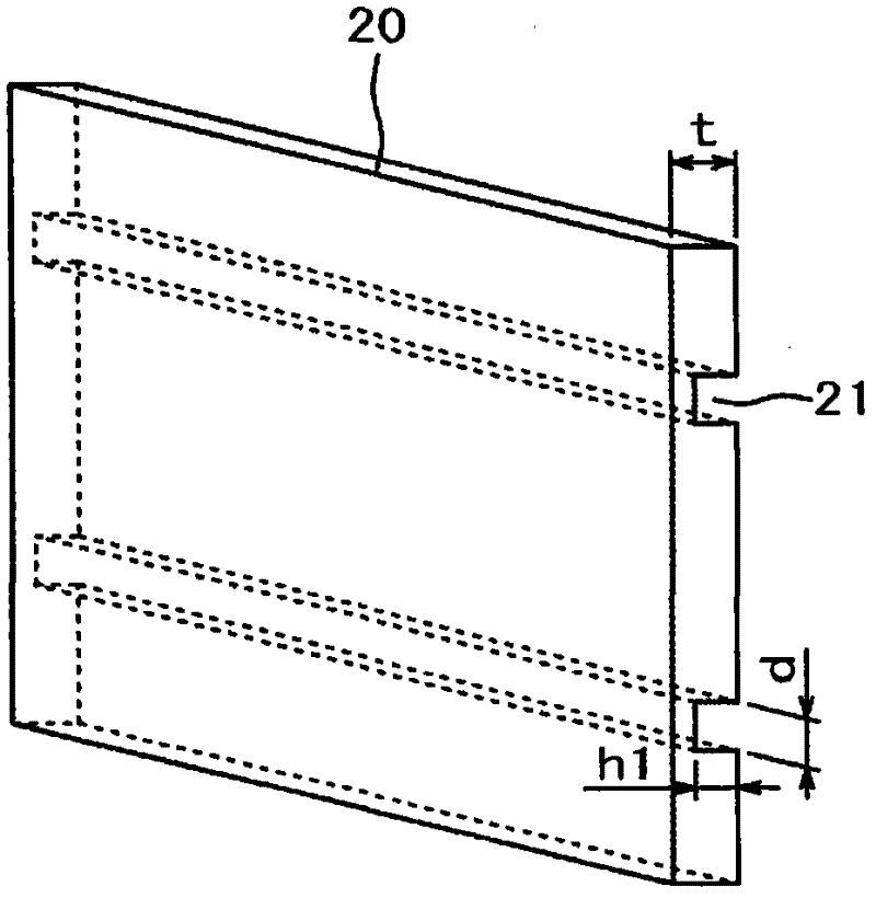
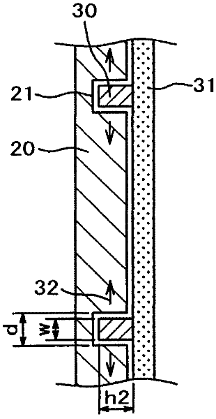
[0098] The structure of the liquid crystal display device and the figure 1 The structure of the description is the same. In addition, the light guide plate 20 used is the same as that used in figure 2 The same as the light guide plate described in . embed figure 2 The LED 30 in the concave portion 21 of the light guide plate 20 shown is a top-view type. Figure 18 A plan view showing a light source embedded in the concave portion 21 of the light guide plate 20 . exist Figure 18 In this case, the wiring substrate 31 made of glass epoxy on which wiring is formed is pasted on both sides of the Al substrate 35 . LED30 is arrange|positioned on the wiring board 31. As shown in FIG. Such a stru...
PUM
 Abstract
Description
Claims
Application Information


