
Memory

A memory and storage area technology, applied in the field of memory, can solve problems such as inability to optimize memory read time and speed, high power consumption, and difficulty in memory wiring, so as to optimize read time and speed, reduce power consumption, and optimize read the effect of time

Active Publication Date: 2011-09-21
SHANGHAI HUAHONG GRACE SEMICON MFG CORP
View PDF5 Cites 0 Cited by
  • Summary
  • Abstract
  • Description
  • Claims
  • Application Information

AI Technical Summary

Problems solved by technology

[0008] Another problem solved by the present invention is the problem of difficult memory wiring when the row decoder drivers have the same size, or if the row decoder drivers have different sizes, the reading time and speed of the memory cannot be optimized, and the problem of high power consumption

Method used


Image

  • Memory
  • Memory
  • Memory

Examples


Embodiment Construction

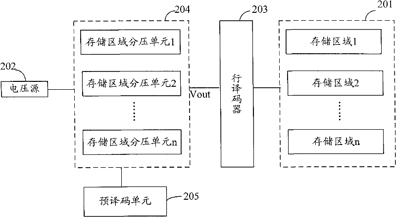
[0027] The memory of the prior art provides the same read voltage to all memory arrays, however, the read characteristics of the memory cells (Cell) of different memory arrays (Array) are not the same, and the actual required read voltage is also different. Similarly, in order to be able to read the data of all storage arrays, it is necessary to provide a higher reading voltage to meet the requirements of the reading voltage of all storage arrays, which will cause high power consumption and slow reading speed of the memory; In the memory according to the specific embodiment of the invention, the storage area voltage dividing unit divides the reading reference voltage provided by the voltage source and provides it as a reading voltage to the corresponding storage area, and each storage area corresponds to a storage area voltage dividing unit, which can be used according to different The read characteristics of the memory cells in the storage area, respectively, divide the voltag...


PUM


Abstract

The invention provides a memory. The memory comprises a plurality of memory regions, a voltage source, a voltage dividing unit and a precoding unit, wherein the voltage source is used for providing the read reference voltage to the memory regions; the voltage dividing unit comprises a plurality of memory region voltage dividing units corresponding to the memory regions; the precoding unit is connected with the voltage dividing unit and is used for selecting the corresponding memory region voltage dividing units according to the address signals input into the precoding unit; and the selected memory region voltage dividing units are used for outputting the divided read reference voltage as the read voltage provided to the corresponding memory regions after dividing the read reference voltage provided by the voltage source. The memory has the following advantages: the power consumption of the memory is reduced and the reading time of the memory can be optimized; and besides, crosstalk between the adjacent memory regions can be avoided from being easily caused when data of some memory regions are read for a long time.

Description

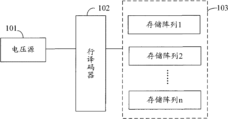
technical field [0001] The present invention relates to the field of memory, in particular to flash memory. Background technique [0002] In recent years, with the rapid development of semiconductor memory, advanced memories such as DRAM, EEPROM, and flash memory have been widely used due to their advantages of high density, low power consumption, and low price. [0003] figure 1 For the structural schematic diagram of the existing memory displaying the reading method, refer to figure 1 , the existing memory includes several storage arrays 103, which are respectively storage array 1, storage array 2...storage array n; row decoder 102, connected with the plurality of storage arrays 101; voltage source 101, in the prior art The voltage source is generally a voltage regulator (Regulator), which is connected to the row decoder 102. When reading the data stored in the memory, the voltage source 101 provides a read value to the corresponding memory array through the row decoder ...

Claims


Application Information

Patent Timeline
Patent Type & Authority Applications(China)
IPC IPC(8): G11C16/06G11C16/08
Inventor 杨光军肖军
Owner SHANGHAI HUAHONG GRACE SEMICON MFG CORP
Learn More