Semiconductor packaging device with resin material loading photoelectric detection device

A technology for photoelectric detection and packaging equipment, which is applied in semiconductor/solid-state device manufacturing, circuits, electrical components, etc. It can solve the problems of high use cost and complex resin structure, and achieve the effect of saving manufacturing cost and use cost, and simple and practical structure

Active Publication Date: 2011-09-21
TONGLING TRINITY TECH
View PDF5 Cites 0 Cited by
  • Summary
  • Abstract
  • Description
  • Claims
  • Application Information

AI Technical Summary

Problems solved by technology

[0003] The purpose of the present invention is to solve the problem of complex structure and hi

Method used


Image

  • Semiconductor packaging device with resin material loading photoelectric detection device
  • Semiconductor packaging device with resin material loading photoelectric detection device
  • Semiconductor packaging device with resin material loading photoelectric detection device

Examples


Embodiment Construction

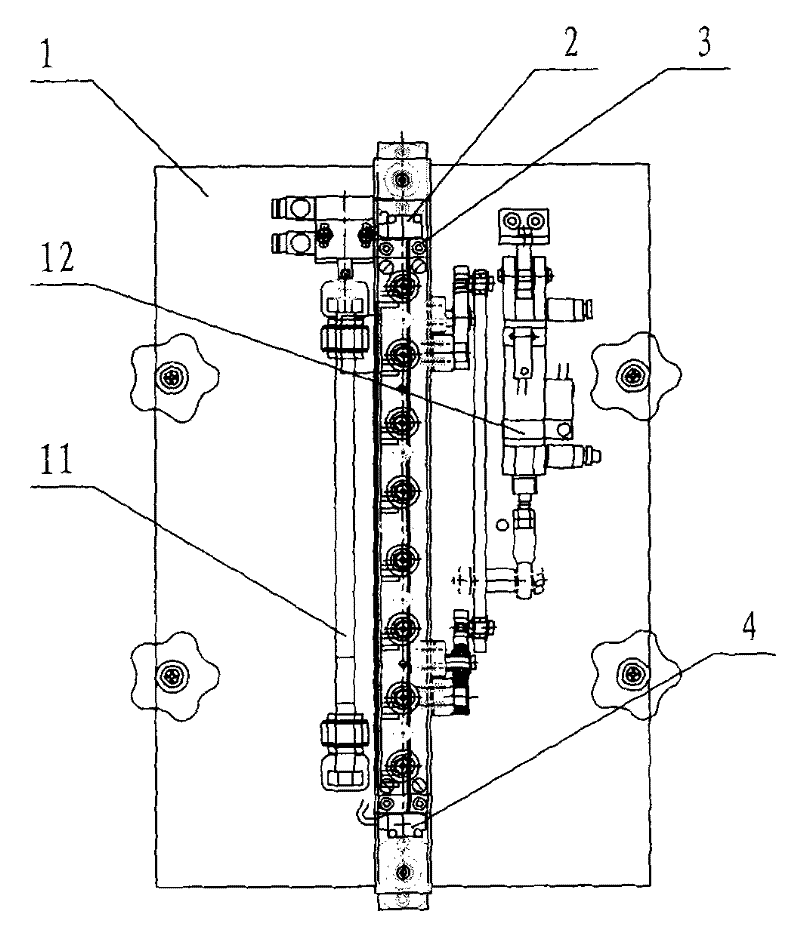
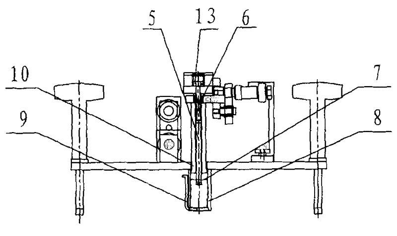
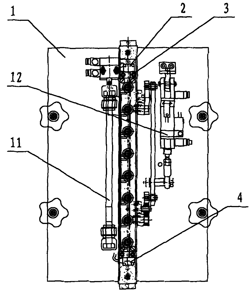
[0010] The present invention is a semiconductor packaging device with a photoelectric detection device for resin feeding, which includes a support plate 1, a resin push-out mechanism 12 and a resin baffle mechanism 11 fixed on the support plate 1, and a storage device located under the support plate 1 for storing The resin seat 8 of the resin 7, and the resin baffle plate 9 used to block the resin 7, are connected with the resin push-out mechanism and connected to several push tubes 10 for pushing the resin 7 through the support plate 1 and extending into the resin seat 8, It is characterized in that it also includes a resin feeding photoelectric detection device fixed on the support plate.

[0011] The photoelectric detection device for resin feeding comprises a photoelectric emission sensor 2, a photoelectric receiving sensor 4 adapted to the photoelectric emission sensor 2, several thimbles 5 and a strip-shaped emission channel plate 3 positioned in the push tube 10, and the...


PUM


Abstract

The invention discloses a semiconductor packaging device with a resin material loading photoelectric detection device. The semiconductor packaging device comprises a support plate [1], a resin seat [8] positioned below the support plate [1] and the resin material loading photoelectric detection device fixed on the support plate. By utilizing the semiconductor packaging device, the manufacturing cost and use cost of the device can be greatly saved, and the semiconductor packaging device is not limited by the quantity of the resin, and has a simple and practical structure.

Description

technical field [0001] The invention relates to semiconductor packaging equipment, especially semiconductor packaging equipment with a photoelectric detection device for resin feeding. Background technique [0002] During the automatic resin feeding process of semiconductor packaging equipment, the resin lifting mechanism of the feeding manipulator transports the arranged resin to the feeding manipulator. The latter keeps the resin in the resin seat by blocking the baffle, and the next step is to put the resin material into the resin barrel in the semiconductor plastic packaging mold. The situation of the resin in the resin seat must be checked before putting it in, which is convenient for deciding the next step of the manipulator action, and prevents the lead frame package from being unqualified due to incorrect or no positioning of the resin material. In order to solve this problem, the known method is to set multiple sensors for detection according to the size and quanti...

Claims


Application Information

Patent Timeline
IPC IPC(8): H01L21/56H01L21/00
Inventor 黄磊赵仁家周小飞陈昌太刘勇杨亚萍
Owner TONGLING TRINITY TECH
Why Eureka
Try Eureka