Plasma processing apparatus
A plasma and processing device technology, which is applied in the field of plasma processing devices, can solve problems such as uneven plasma processing, and achieve the effect of improving the degree of freedom of adjustment and improving uniformity
- Summary
- Abstract
- Description
- Claims
- Application Information
AI Technical Summary
Problems solved by technology
Method used
Image
Examples
no. 1 approach
[0038] [First embodiment: square coil, common power supply]
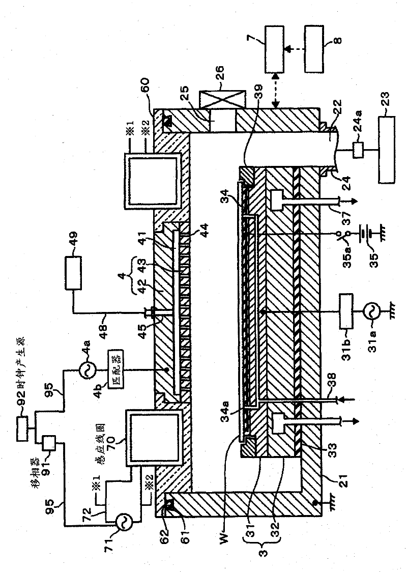
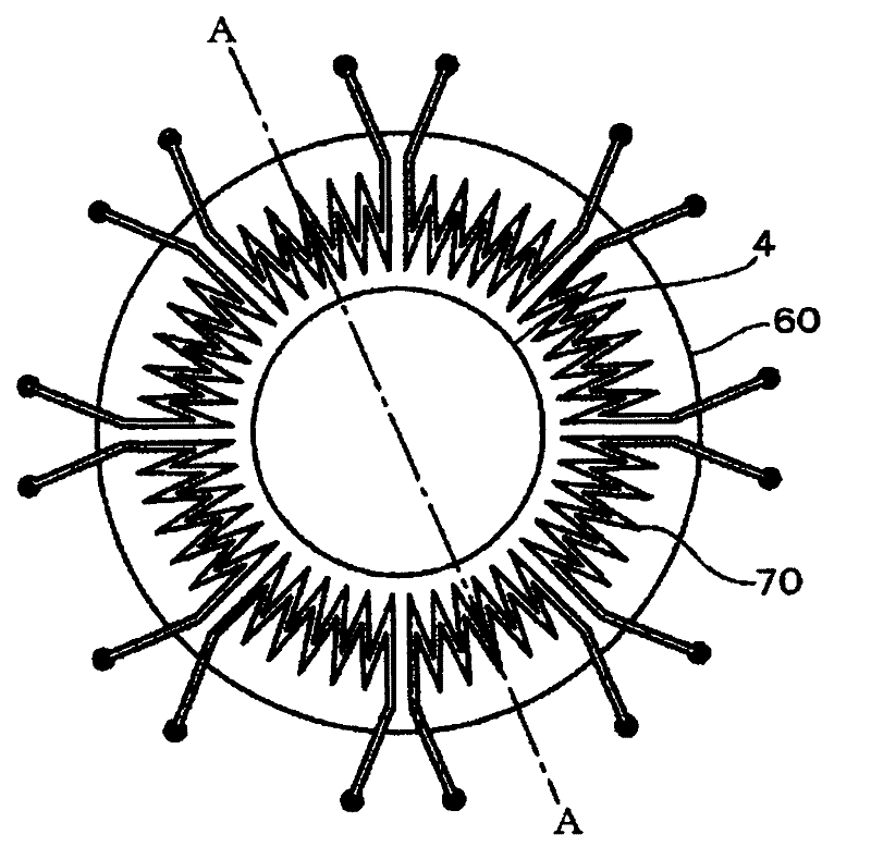
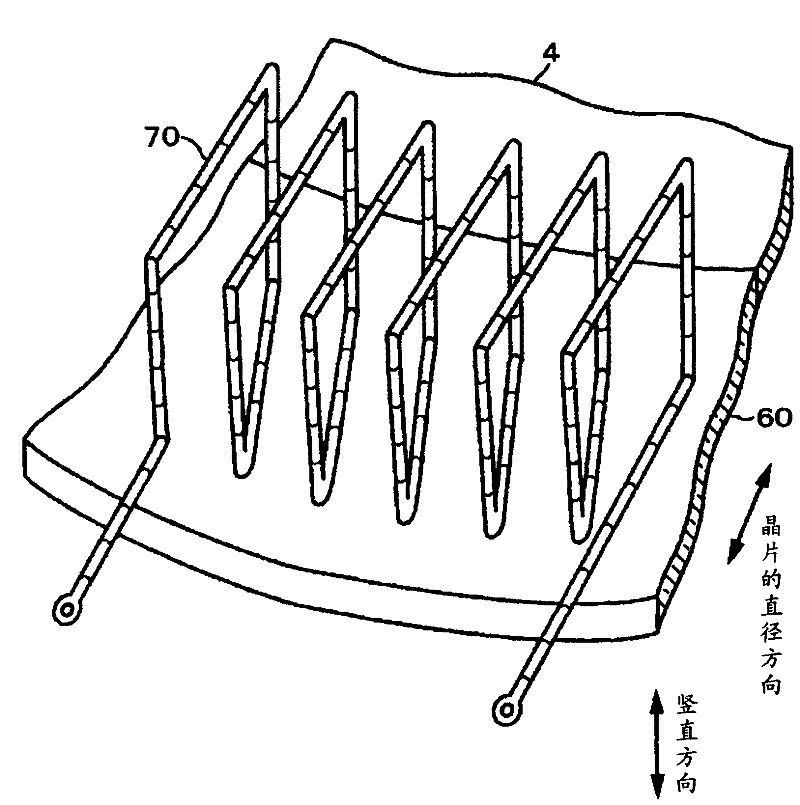
[0039] refer to Figure 1 ~ Figure 4 A first embodiment in which the plasma processing apparatus of the present invention is applied as a plasma etching apparatus will be described. This plasma etching processing apparatus includes a processing container 21 constituted by a vacuum chamber, and a mounting table 3 arranged in the center of the bottom surface of the processing container 21 . The processing container 21 is electrically grounded, and an exhaust port 22 is formed at a position lateral to the mounting table 3 on the bottom surface of the processing container 21 . The exhaust port 22 is connected to a vacuum exhaust unit 23 including a vacuum pump or the like via an exhaust pipe 24 provided with a pressure adjustment valve 24 a as a pressure adjustment unit. A transfer port 25 for loading and unloading the wafer W is provided on a side wall of the processing container 21 , and the transfer port 25 is conf...
no. 2 approach
[0065] [Second Embodiment: Planar Coil, Shared Power Supply]
[0066] In the above-mentioned first embodiment, the square induction coil 70 was described, but in this second embodiment, in order to form the second electric field E2, for example, Figure 12 As shown, a plurality of linear conductive wires 111 are arranged radially over the entire circumferential direction. In this second embodiment, if Figure 12 As shown in (b), a plurality of conductive wires 111 are embedded in an annular flat plate 112 made of, for example, a dielectric material in such a manner that the inner and outer peripheral sides of the conductive wires 111 are exposed, and the flat plate 112 and the plurality of conductive wires 111 are It is installed on the outer top plate 60 .
[0067] In addition, in order to connect the conduction path 72 so that the impedance between the plurality of lead wires 111 becomes the same value as that of the second high-frequency power supply unit 71, for example,...
no. 3 approach
[0071] [Third Embodiment: Square Coil, Multiple Power Supply]
[0072] In the above-mentioned first embodiment, high frequencies are supplied to the plurality of induction coils 70 from the common second high-frequency power supply unit 71, but in this third embodiment, for example, Figure 15 As shown, the second high-frequency power supply unit 71 is connected to each induction coil 70 . Also in this case, the respective conductive paths 72 are set to have the same length so that the impedances between the respective second high-frequency power supply units 71 and the respective induction coils 70 have the same value. In addition, for the common phase shifter 91 connected to these multiple second high-frequency power supply units 71, the signal path 95 is set to the same length so that the phase shifter 91 and these multiple second high-frequency power supply units 71 The impedance between is the same value.
[0073] In this device, the plasma etching process can be perfor...
PUM
 Abstract
Description
Claims
Application Information
 - R&D
- Intellectual Property
- Life Sciences
- Materials
- Tech Scout
- Unparalleled Data Quality
- Higher Quality Content
- 60% Fewer Hallucinations
Browse by: Latest US Patents, China's latest patents, Technical Efficacy Thesaurus, Application Domain, Technology Topic, Popular Technical Reports.
© 2025 PatSnap. All rights reserved.Legal|Privacy policy|Modern Slavery Act Transparency Statement|Sitemap|About US| Contact US: help@patsnap.com


