Array antenna and manufacturing method thereof

A technology of array antennas and antenna elements, which is applied to antennas, individually powered antenna arrays, electrical components, etc., to achieve the effect of reducing useless radiation

Inactive Publication Date: 2011-12-28
NEC CORP
View PDF7 Cites 2 Cited by
  • Summary
  • Abstract
  • Description
  • Claims
  • Application Information

AI Technical Summary

Problems solved by technology

Therefore, the unwanted radiation of the microstrip line has a great influence on the side lobe characteristics of the array antenna

Method used


Image

  • Array antenna and manufacturing method thereof
  • Array antenna and manufacturing method thereof
  • Array antenna and manufacturing method thereof

Examples


no. 1 approach

[0045] A first embodiment for carrying out the present invention will be described in detail with reference to the drawings.

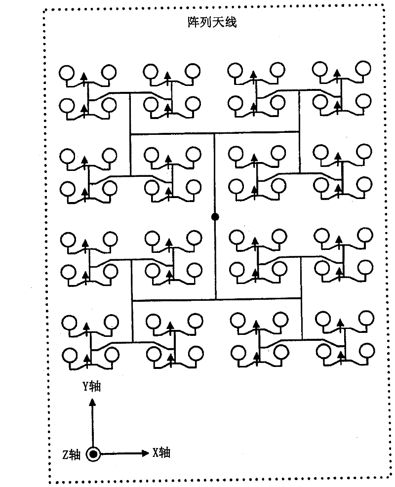
[0046] Figure 5 It is a circuit diagram showing the configuration of the array antenna 1 of this embodiment. Referring to this figure, array antenna 1 has a plurality of antenna elements A1, A2, etc., and a power supply circuit.

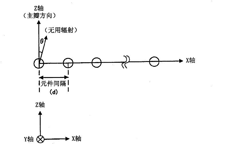
[0047] In this figure, an X-Y plane including an X-axis and a Y-axis is parallel to the paper surface, and a Z-axis is in a direction perpendicular to the X-Y plane. Moreover, all the antenna elements and the lines of the power supply circuit are arranged on the printed circuit board on the X-Y plane. For example, this Z-axis direction is set as the main lobe direction of the array antenna 1 .

[0048] In order to reduce the loss, the printed circuit board is suitable to use PTFE (Polytetrafluoroethylene) as the material, but for the purpose of reducing the material cost, BT (bismaleimide triazine, Bismaleimide-Triazine) ...

no. 2 approach

[0069] refer to Figure 9 A second embodiment of the present invention will be described. This figure is a circuit diagram showing the configuration of the array antenna 1a of this embodiment. Referring to this figure, the antenna elements and microstrip lines of this embodiment are divided into four groups (first to fourth subarrays).

[0070] If the offset of the second sub-array relative to the first sub-array is set to δ, then the offset of the third sub-array relative to the first sub-array is twice that of the fourth sub-array relative to the first sub-array. is offset by three times that.

[0071] If the offset of the second subarray relative to the first subarray and the offset of the fourth subarray relative to the first subarray are the same value, then the X coordinates of the unwanted radiation wave sources in the second and fourth subarrays Same, no offset. However, in this embodiment, the offsets of the sub-arrays other than the first sub-array relative to th...

no. 3 approach

[0073] refer to Figure 10 A third embodiment of the present invention will be described. This figure is a circuit diagram showing the configuration of the array antenna 1b of this embodiment. Referring to this figure, in the array antenna 1b, the sub-arrays are shifted in each column along the arrangement direction.

[0074] According to the configuration of the array antenna 1 of the first embodiment, if the offset is performed every two columns, the columns in each sub-array will not be offset. However, as shown in the configuration of the present embodiment, when offset is performed for each column, the sources of unwanted radiation of each column are dispersed, further degrading the side lobe characteristics.


PUM


Abstract

An array antenna has: a plurality of first antenna elements arranged at predetermined element intervals on the flat surface of a substrate; a plurality of second antenna elements arranged at the element intervals in parallel to the arrangement direction of the first antenna elements on the flat surface; a first power supply circuit which supplies power to each of the first antenna elements by means of lines branched at a first branching point on the flat surface; and a second power supply circuit which supplies power to each of the second antenna elements by means of lines branched at a second branching point shifted from the first branching point by a predetermined distance in the arrangement direction on the flat surface.

Description

technical field [0001] The present invention relates to a technique for improving the side lobe characteristics of an array antenna. Background technique [0002] In wireless systems such as point-to-point systems, for example parabolic antennas or array antennas are used. [0003] Such as figure 1 As shown, a general array antenna is composed of a plurality of antenna elements provided on a printed circuit board, and a power supply circuit for supplying power to the antenna elements. The circles in this figure are antenna elements, and the solid lines connecting the antenna elements are lines (microstrip lines) constituting a power supply circuit. As shown in the figure, the antenna elements are arranged in a dot matrix on the printed circuit board. [0004] In the array antenna having the above configuration, useless radiation (grating lobes) is generated on the printed circuit board in a direction different from the maximum radiation direction (main lobe direction). I...

Claims


Application Information

Patent Timeline
Patent Type & Authority Applications(China)
IPC IPC(8): H01Q21/06H01Q13/08
CPCH01Q21/06Y10T29/49016
Inventor 田边浩介大嶋笃司
Owner NEC CORP
Why Eureka
Try Eureka