Plasma display panel display device

a display device and display panel technology, applied in the direction of identification means, instruments, electric discharge tubes, etc., can solve the problems of unwanted radiation, difficult to reduce unwanted radiation with these devices, and difficult to cancel out the magnetic field components generated in the device sufficiently, so as to reduce unwanted radiation

Inactive Publication Date: 2009-06-04
PANASONIC CORP
View PDF2 Cites 0 Cited by
  • Summary
  • Abstract
  • Description
  • Claims
  • Application Information

AI Technical Summary

Benefits of technology

[0021]In the present invention, the plasma display panel and the first through third conductive members have substantially the same width and height, and interconnections are made in the end portions of these elements, so as to cancel out the magnetic field components generated between the plasma display panel and the first conductive member, and between the second conductive member and the third conductive member. The present invention therefore sufficiently reduces unwanted radiation in the plasma display panel display device.

Problems solved by technology

The large current in the loop generates a strong magnetic field, which is the primary cause of unwanted radiation in the display device.
However, it is difficult to reduce unwanted radiation sufficiently with these devices.
Regarding the first device, as shown in FIG. 6, since the connector cable is considerably narrower in height than the plasma display panel, the magnetic flux generated from the first loop and the magnetic flux generated from the second loop originate and terminate at different heights (vertical positions in FIG. 6), making it difficult to cancel out the magnetic field components generated in the device sufficiently.
In the second device, because the first and second current loops are formed by dividing the current from the plasma display panel, it is difficult to create the same current intensity in these current loops.
Accordingly, it is difficult to cancel out the magnetic field components generated in the device sufficiently.

Method used


Image

  • Plasma display panel display device
  • Plasma display panel display device
  • Plasma display panel display device

Examples


first embodiment

[0030]With reference to FIG. 1 and FIG. 5, the following will describe an embodiment (First Embodiment) of a plasma display panel display device of the present invention.

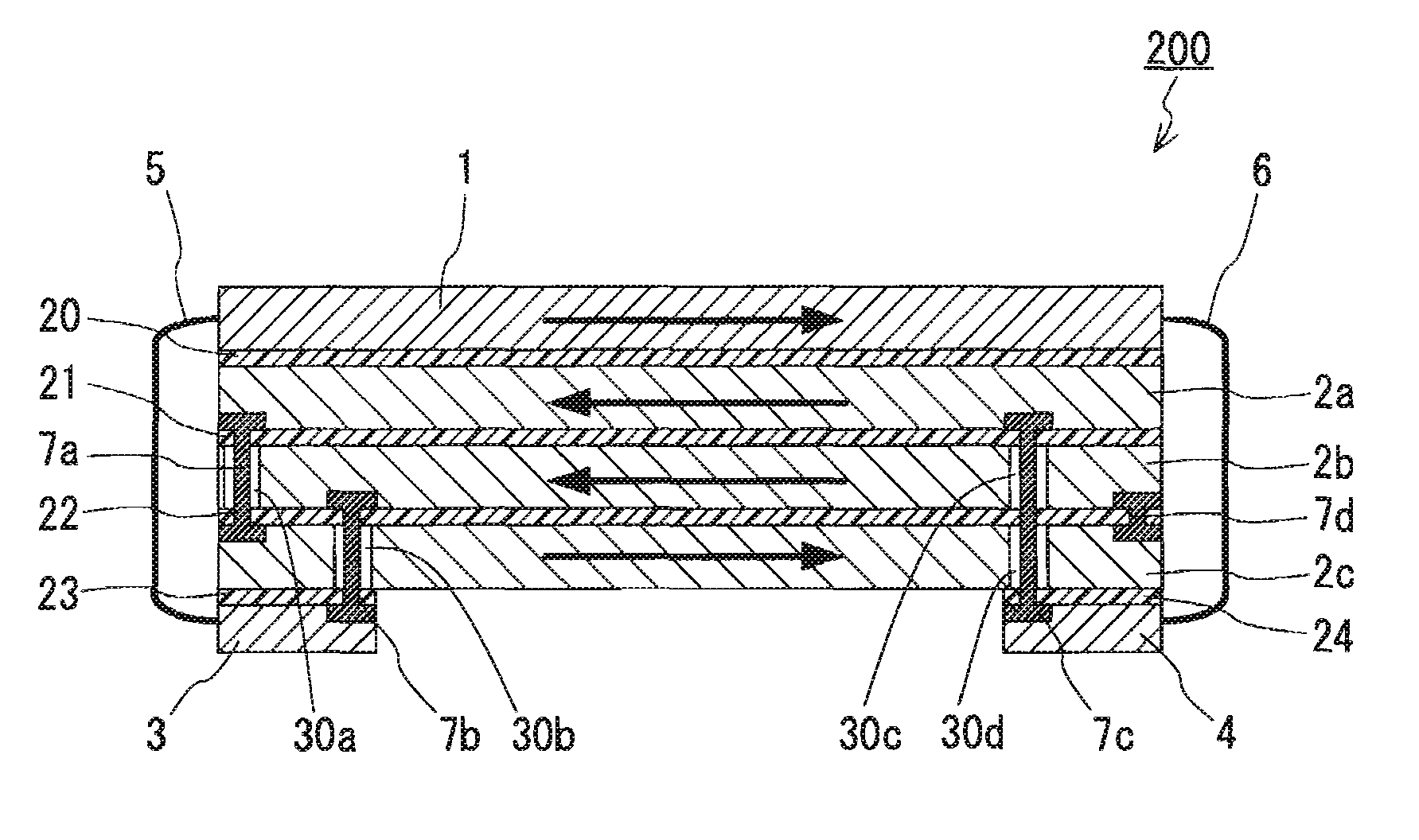
[0031]FIG. 5 is a perspective view of a plasma display panel display device of the present invention. FIG. 1 is a lateral cross sectional view of the display device shown in FIG. 5.

[0032]As shown in FIG. 1, a display device 200 includes: a plasma display panel (front panel) 1 to display an image; a first conductive member 2a; a second conductive member 2b; a third conductive member 2c; a substrate 3 provided with an X electrode driving circuit; a substrate 4 provided with a Y electrode driving circuit; flexible wiring substrates 5 and 6; conductors (joint members) 7a, 7b, 7c, and 7d; and insulating layers 20, 21, 22, 23, and 24. The first through third conductive members 2a, 2b, and 2c are provided as aluminum chassis.

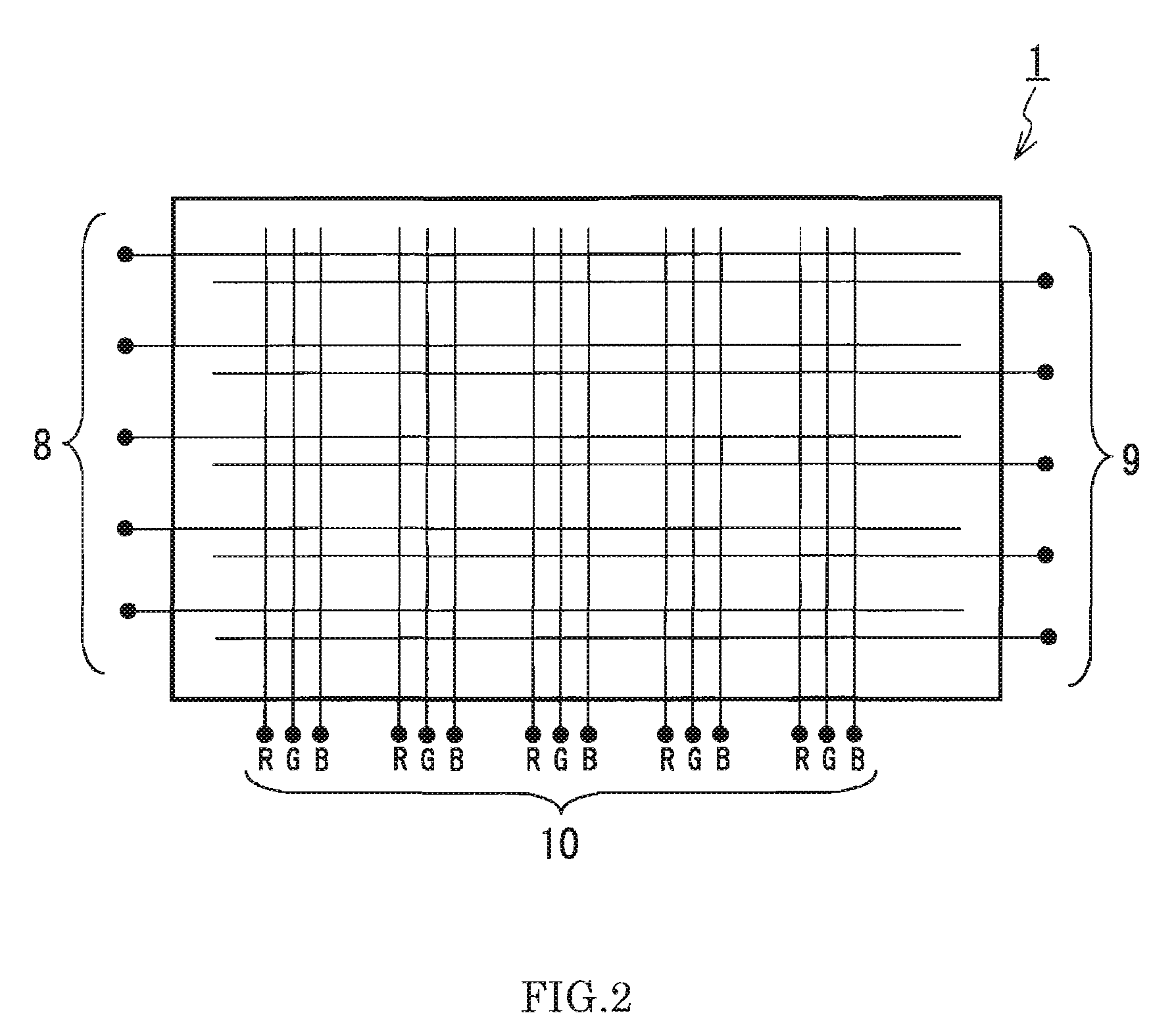
[0033]The front panel 1 can be realized by a known plasma display panel. FIG. 2 is a diagram explai...

second embodiment

[0061]The following will describe another embodiment (Second Embodiment) of a plasma display panel display device of the present invention, with reference to FIG. 3.

[0062]FIG. 3 is a lateral cross sectional view of another example of a plasma display panel display device of the present invention. A display device 300 according to the Second Embodiment of the present invention has the same structure as the display device 200 of the First Embodiment, except for the manner in which the interconnections are made by the joint members. As shown in FIG. 3, the display device 300 is structured to include: a joint member 7e electrically connecting the second conductive member 2b and the third conductive member 2c in the left end portion of these members; a joint member 7f electrically connecting the ground of the X electrode driving circuit to the first conductive member 2a in the left end portion of the first conductive member 2a; a joint member 7g electrically connecting the ground of the ...


PUM


Abstract

The present invention sufficiently reduces unwanted radiation in a plasma display panel (PDP) display device. The display device includes a PDP having a pair of electrodes, a first, a second, and a third conductive member, and a pair of driving circuits used to apply a voltage to their respective electrodes. Each conductive member has substantially the same width and height as the PDP, and the first, second, third conductive members are disposed on the rear surface of the PDP, in this order on the rear side of the PDP. The PDP and the conductive members are connected electrically to one another in the end portions of these elements, either directly or via the driving circuits, so that the direction of the current flowing in the PDP during driving and discharge coincides with the direction of the current flowing in the third conductive member, and is opposite from the direction of the current flowing in the first conductive member and the second conductive member.

Description

BACKGROUND OF THE INVENTION[0001]1. Field of the Invention[0002]The present invention relates to plasma display panel display devices, and particularly a plasma display panel display device capable of reducing unwanted radiations that occur during the driving and discharge of a plasma display panel.[0003]2. Description of Related Art[0004]Because of advantages including a large screen size and a thin screen, plasma display panel display devices have been well-spread in recent years.[0005]With reference to FIG. 4, conventional plasma display panel display devices are described below in regard to structure and image display operation. FIG. 4 is a lateral cross sectional view showing a schematic illustration of a structure of a conventional plasma display panel display device 100. As shown in FIG. 4, the display device 100 includes a plasma display panel (front panel) 1 that forms an image.[0006]The plasma display panel 1 includes sustain discharge electrodes (hereinafter “X electrodes...

Claims


Application Information

Patent Timeline
Patent Type & Authority Applications(United States)
IPC IPC(8): G09G3/28G09F9/00
CPCG09G3/296H01J2211/446H01J11/44G09G2330/06
Inventor ICHIKAWA, KEIFUSAYASU, HIROTSUGUKUNIMOTO, HIROSHIHAMADA, SEIJIMATSUBARA, RYO
Owner PANASONIC CORP
Why Eureka
Try Eureka