Clock generation circuit, and communication device

A clock generation circuit and additional circuit technology, applied in the direction of generating/distributing signals, electrical components, pulse position modulation, etc., can solve the problems of wireless communication influence, misoperation of surrounding circuit electronic equipment, etc., and achieve the effect of reducing useless radiation

Inactive Publication Date: 2007-05-30
ROHM CO LTD
View PDF2 Cites 10 Cited by
  • Summary
  • Abstract
  • Description
  • Claims
  • Application Information

AI Technical Summary

Problems solved by technology

As a result, electromagnetic waves radiated from the clock generation circuit are generated, causing malfunctions of peripheral circuits or other electronic equipment, or affecting wireless communication, etc.

Method used


Image

  • Clock generation circuit, and communication device
  • Clock generation circuit, and communication device
  • Clock generation circuit, and communication device

Examples


no. 1 Embodiment approach

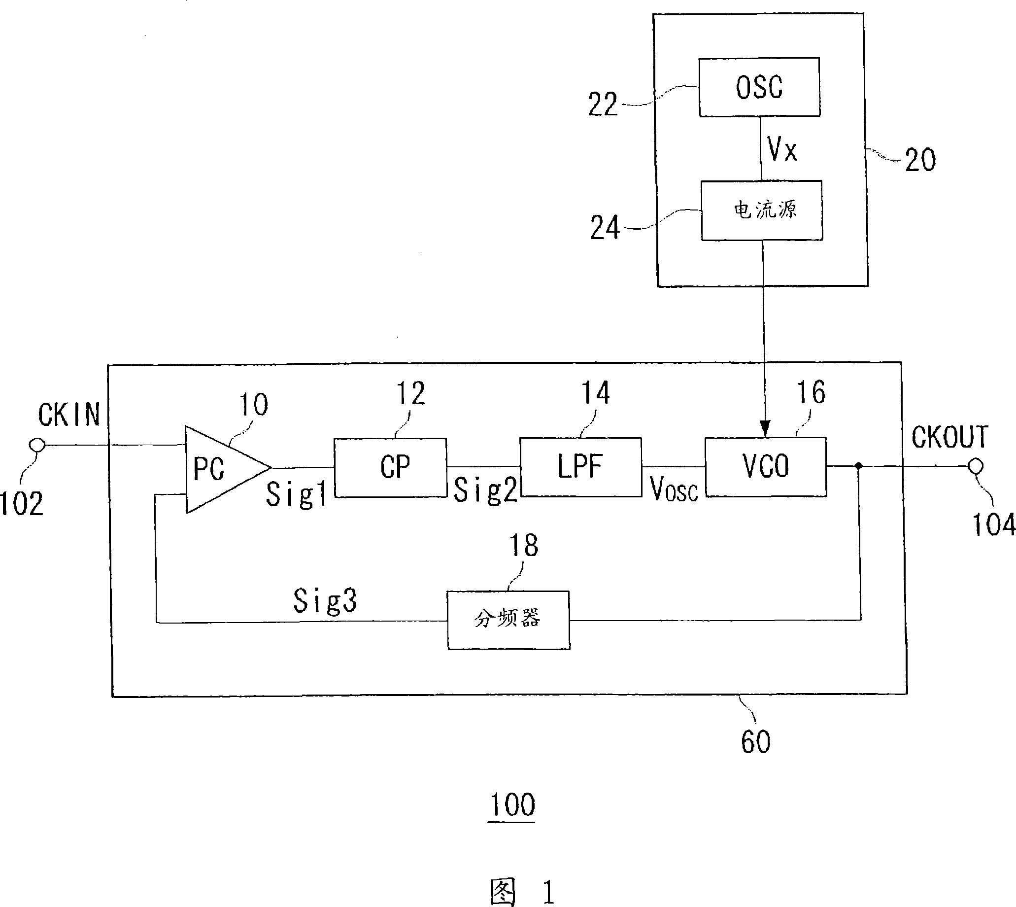
[0048] FIG. 1 shows the configuration of a clock generating circuit 100 in the first embodiment of the present invention.

[0049] The clock generation circuit 100 includes an input terminal 102 and an output terminal 104 . The signals input or output to the respective terminals are respectively referred to as an input clock signal CKIN and an output clock signal CKOUT. The frequencies of the input clock signal CKIN and the output clock signal CKOUT are referred to as input clock frequency fIN and output clock frequency fOUT, respectively.

[0050] This clock generating circuit 100 includes a PLL circuit 60 and a jitter adding circuit 20 .

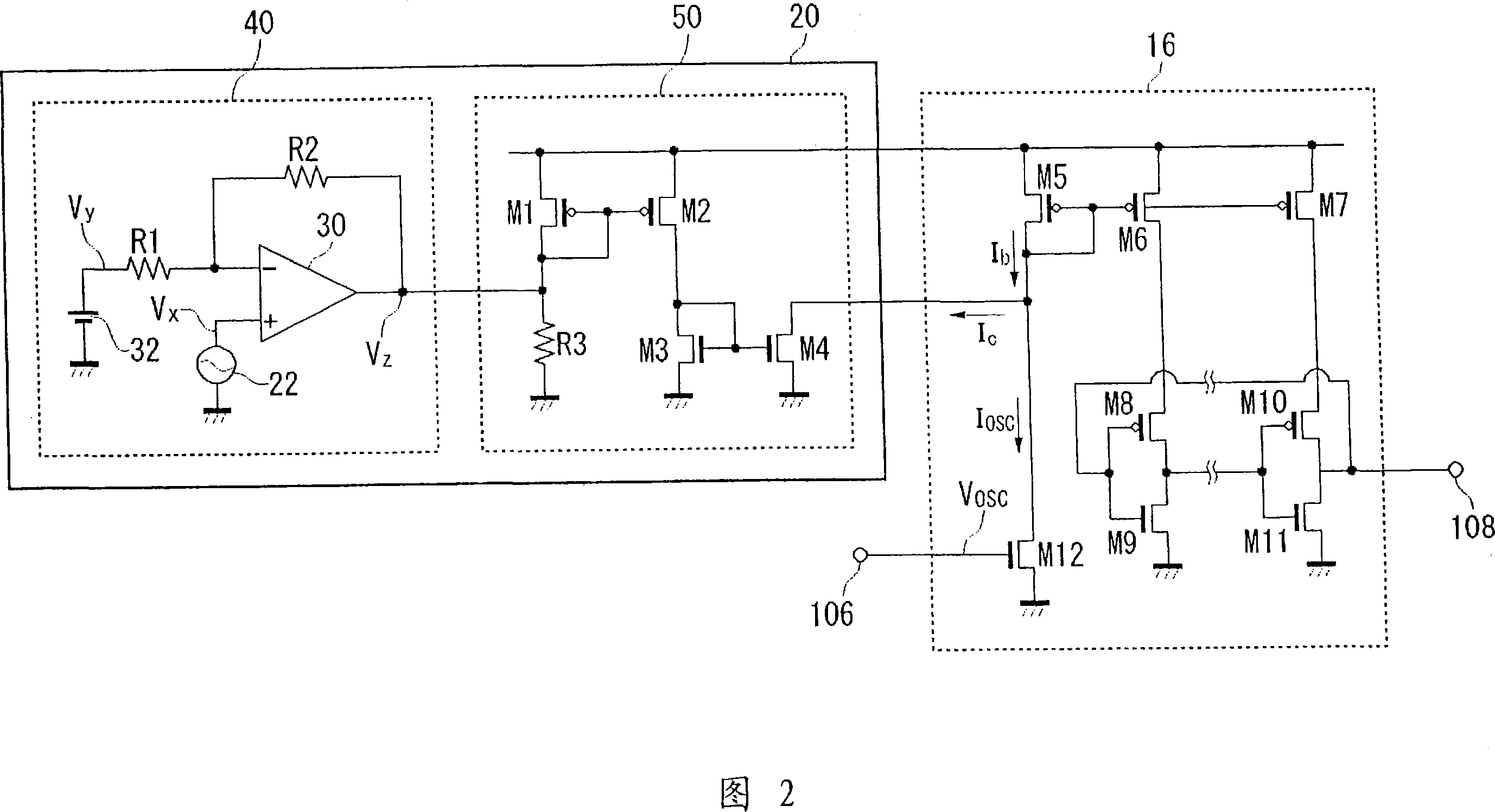
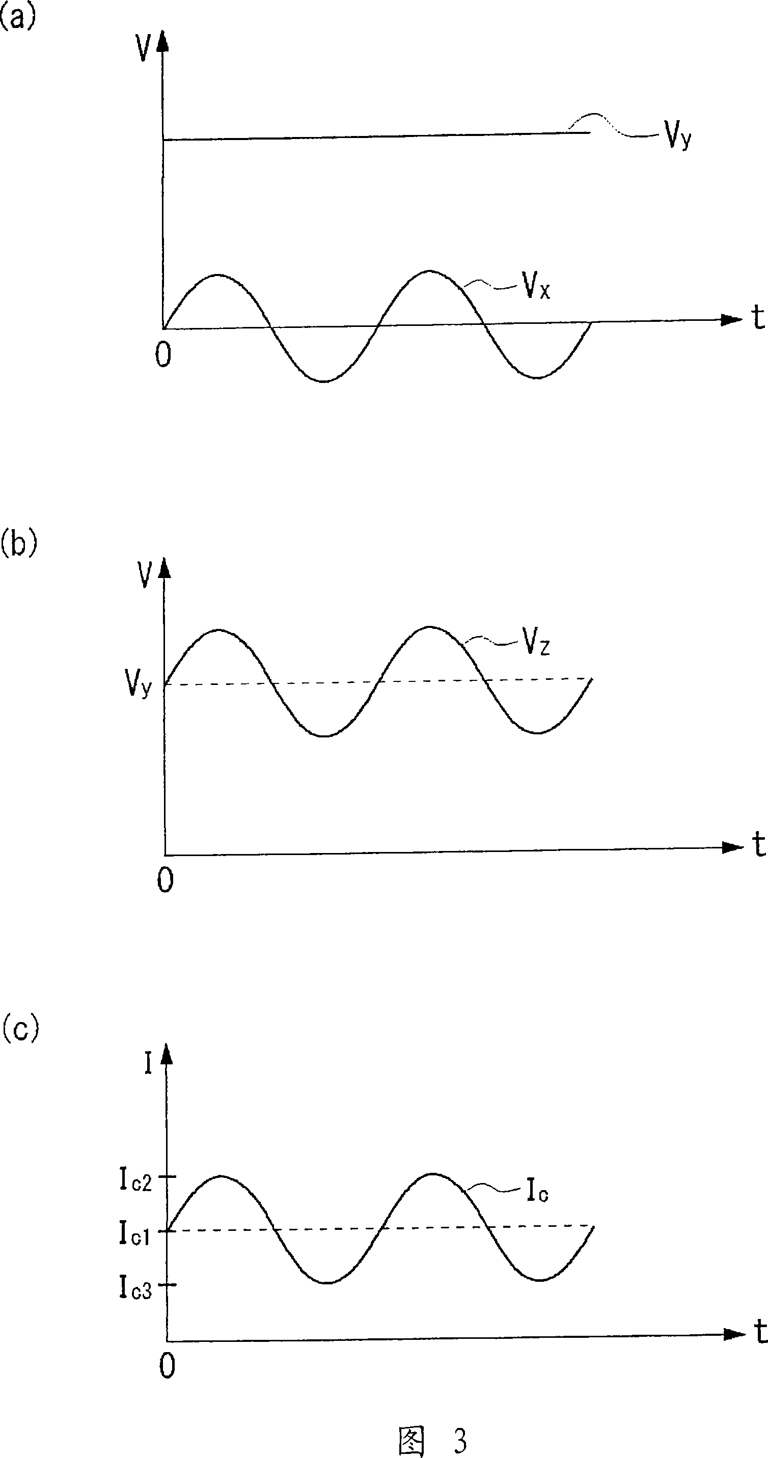
[0051] The PLL circuit 60 includes a phase comparator 10 , a charge pump circuit 12 , a low-pass filter 14 , a voltage controlled oscillator 16 , and a frequency divider 18 . The clock generation circuit 100 multiplies the input clock signal CKIN by the frequency division ratio N set by the frequency divider 18 and outputs the clock sign...

no. 2 Embodiment approach

[0082] FIG. 6 is a block diagram showing the configuration of a clock generation circuit 100 according to the second embodiment of the present invention. In FIG. 6 , constituent elements that are the same as or equivalent to those already shown are assigned the same reference numerals, and appropriate descriptions thereof are omitted.

[0083] In the clock generating circuit 100 of the first embodiment, spectrum spreading is performed by varying the bias current of the voltage controlled oscillator 16, but in the clock generating circuit 100 related to the second embodiment shown in FIG. 6 , by Spectrum spreading is performed by adding dither to the oscillation control signal Vosc input to the voltage controlled oscillator 16 .

[0084] The clock generating circuit 100 of the present embodiment includes a jitter adding circuit 20 in the subsequent stage of the low-pass filter 14 . The dither adding circuit 20 includes an adder 70 and an oscillator 72 . The oscillator 72 outp...


PUM


Abstract

A clock generation circuit enabled to adjust the quantity of diffusion of a desired spectrum easily and reduced in unnecessary radiation. A clock generation circuit (100) comprises a PLL circuit (60) and a jitter addition circuit (20). The jitter addition circuit (20) generates a bias current for driving a voltage-controlled oscillator (16) of the PLL circuit (60), and adds fluctuations. This jitter addition circuit (20) includes an oscillator (22) and a current source (24) so that the fluctuation components generated by the oscillator (22) are added to the bias current. The oscillation frequency of the oscillator (22) is several times as high as the natural number of the frequency of an input clock signal (CKIN).

Description

technical field [0001] The invention relates to a clock generation circuit and a communication device using it, in particular to a technique for reducing useless radiation. Background technique [0002] In small information terminals such as mobile phones and PDAs (Personal Digital Assistance), clock generation circuits are used to drive semiconductor devices used inside or to generate high-frequency signals required for wireless communications. The frequency of an output clock signal of such a clock generation circuit is increasing with the increase in speed of small information terminals in recent years. As a result, electromagnetic waves radiated from the clock generating circuit are generated, causing malfunctions of peripheral circuits and other electronic devices, or affecting wireless communication and the like. [0003] Such a problem is known as EMI (Electromagnetic Interference), and as a method of reducing this EMI, a technique of frequency-modulating a clock sig...

Claims


Application Information

Patent Timeline
Patent Type & Authority Applications(China)
IPC IPC(8): H03K7/04G06F1/04H03L7/099H03L7/18
CPCH04B15/02G06F1/04H03L2207/06H03K5/132H03K5/133H03L7/18H03K2005/00032H03L7/0995H04B2215/067
Inventor 杉本泰仁
Owner ROHM CO LTD
Why Eureka
Try Eureka