

LCD (liquid crystal display) seamless splicing system
A seamless splicing and optical system technology, applied in the field of LCD display, can solve problems such as image disorder, high manufacturing process difficulty, and low cost, and achieve the effects of saving costs, eliminating LCD seams, and simplifying design
- Summary
- Abstract
- Description
- Claims
- Application Information
AI Technical Summary
Problems solved by technology
Method used
Image

Examples
Embodiment 1
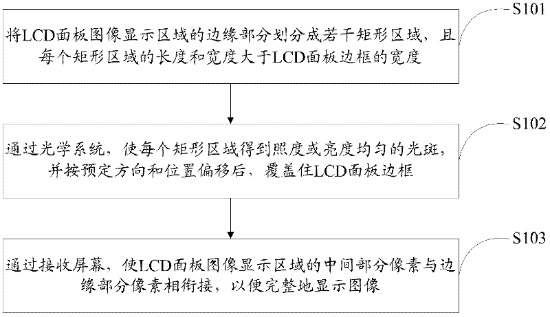
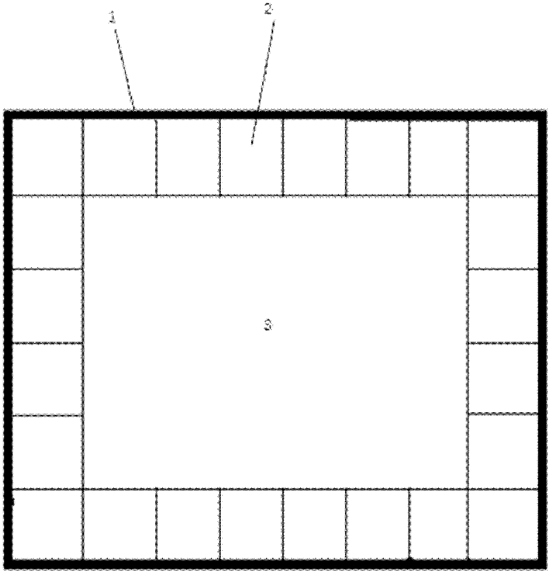
[0045] The optical system structure used in this embodiment and the method for realizing LCD seamless splicing are as follows: Figure 2-9 shown. Such as figure 2 As shown, the image display area of the LCD panel is first divided into the middle part 3 and the edge part, and then the edge part is divided into several identical rectangular areas 2, and the purpose of covering the LCD frame 1 is achieved through the design of the optical system. On this basis, the pixels in the middle part of the image display area of the LCD panel are connected with the pixels in the edge part through the receiving screen, so as to completely display the image.
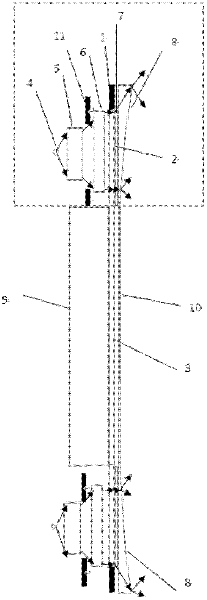
[0046] image 3 Shown is a schematic diagram of the optical system design of this embodiment. The optical system corresponding to the middle part 3 of the LCD panel image display area is a common direct-type LED backlight system 9; the optical system structure corresponding to the edge part of the LCD image display area is as f...
Embodiment 2
[0049] see Figure 10 , this embodiment is the same as the first embodiment except for the following features.
[0050] Such as Figure 10 As shown, the optical system can also omit the design of the offset system, and the purpose of eliminating the frame of the LCD can also be achieved by adjusting the angle of light incident on the LCD panel. Such as Figure 10 As shown, after the light emitted by the light source 4 passes through the uniform light system 5 and the light collimation system 6, the outgoing light forms a certain angle with the normal direction of the LCD panel. By adjusting and receiving the height of the edge portion 8 of the screen as H, the purpose of covering the LCD frame can be achieved. If the width of the LCD frame is L, the angle at which the light needs to be inclined is θ=atan(L / H).
[0051] Such as Figure 10 As shown, an aperture structure 11 is also provided between the light homogenization system and the light collimation system in this embo...
Embodiment 3
[0053] see Figure 11 , this embodiment is the same as the first embodiment except for the following features.
[0054] Such as Figure 11 As shown, the design of the light collimation system 6 and the offset system 7 can also be omitted in this example. Such as Figure 11 As shown, the magnification and offset of the image can be directly carried out by utilizing the property that the light has a certain included angle (the value can be determined according to specific needs) with the normal direction of the LCD panel after passing through the uniform light system 5, so as to reach the final coverage of the frame 1 of the LCD panel. Purpose.
[0055] The LCD seamless splicing system described in the above embodiments is efficient, energy-saving, and compact in structure, and is not only suitable for 1×N-dimensional seamless splicing, but also suitable for N×N (N≥2)-dimensional seamless splicing, and has no loss of pixels. The system structure is easy to realize based on t...
PUM
 Abstract
Description
Claims
Application Information