
Array substrate, liquid crystal display device and manufacturing method for array substrate

A technology of liquid crystal display devices and array substrates, applied in nonlinear optics, instruments, optics, etc., can solve problems affecting display quality, reducing brightness, etc., and achieve the effect of improving the display effect of large viewing angles, increasing brightness, and flexible range

Inactive Publication Date: 2012-04-04
TCL CHINA STAR OPTOELECTRONICS TECH CO LTD
View PDF4 Cites 7 Cited by
  • Summary
  • Abstract
  • Description
  • Claims
  • Application Information

AI Technical Summary

Problems solved by technology

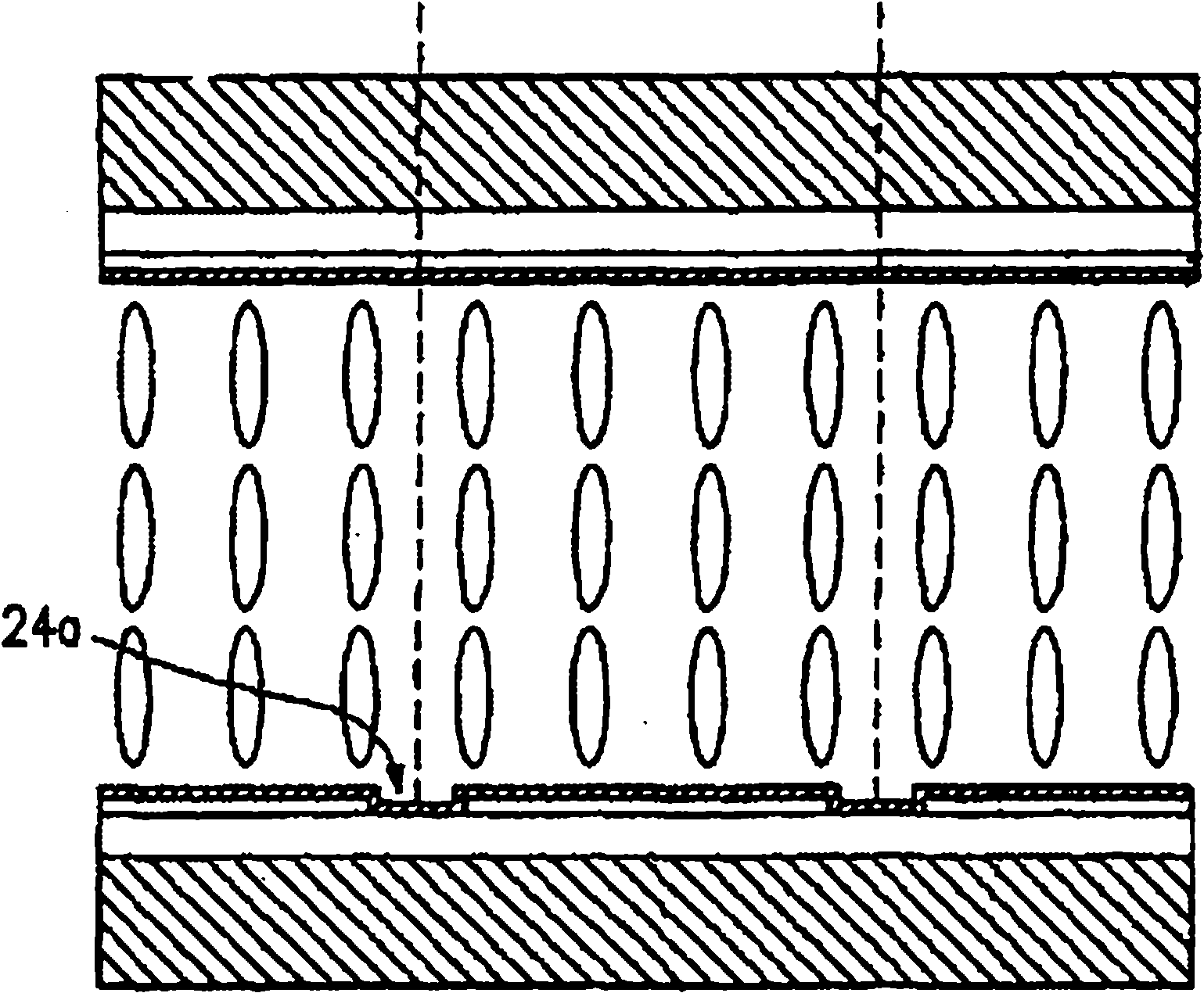
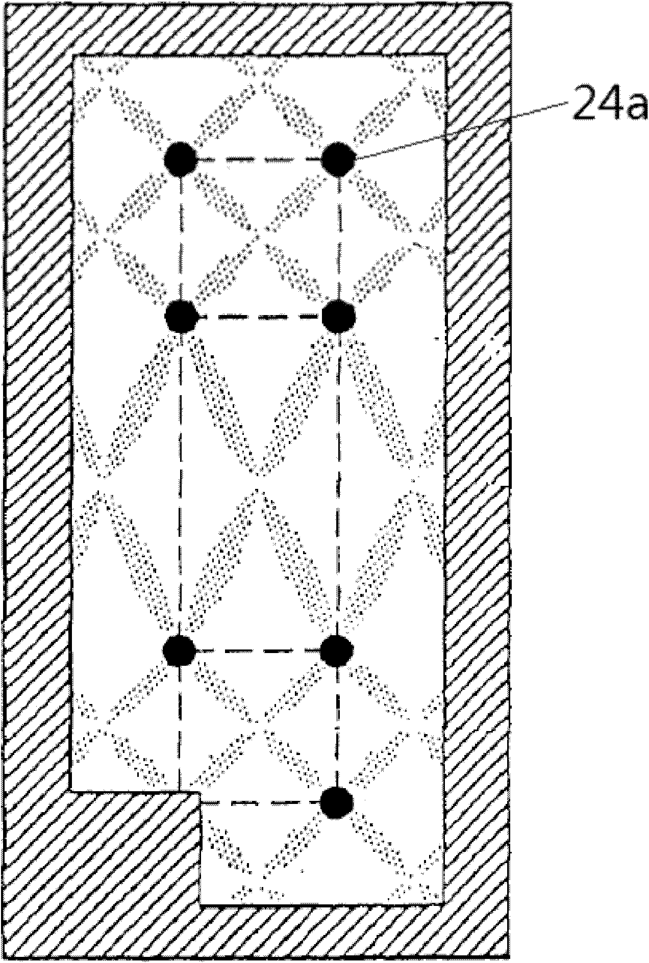
[0003] The defect of this scheme is that the "hole" opening 24a directly cuts off the electrode, so the opening 24a does not function as an electrode. When a voltage is applied to the upper and lower plates, the electric field at the center of the opening 24a is almost zero, so the liquid crystal molecules Basically perpendicular to the array substrate, it will appear as figure 2 The black point shown, reduces the brightness and affects the display quality

Method used


Image

  • Array substrate, liquid crystal display device and manufacturing method for array substrate
  • Array substrate, liquid crystal display device and manufacturing method for array substrate
  • Array substrate, liquid crystal display device and manufacturing method for array substrate

Examples


Embodiment 1

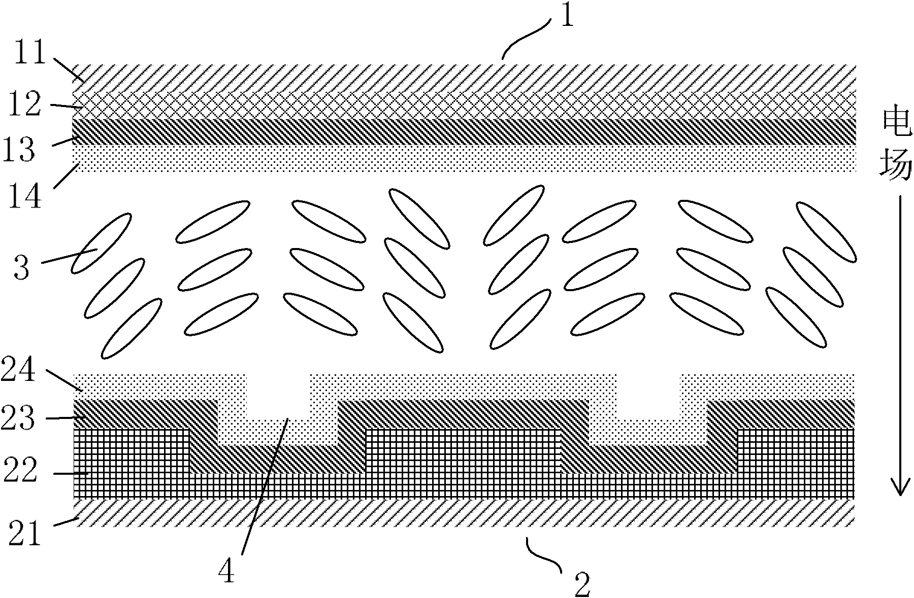
[0032] Embodiment one: if image 3 As shown, the array substrate 2 includes a first transparent substrate 21, a first insulating layer 22 covering the surface of the first transparent substrate 21, an electrode layer covering the surface of the first insulating layer 22 formed with a plurality of pixel electrodes 23, The first alignment film 24 covering the surface of the pixel electrode 23; the color filter substrate 1 includes a second transparent substrate 11, a color filter plate 12 covering the surface of the second transparent substrate 11, and a counter electrode covering the surface of the color filter plate 12 13. A second alignment film 14 covering the surface of the counter electrode 13 . There are multiple recessed regions on the first insulating layer 22 , and correspondingly, the electrode layer and the first alignment film 24 are also recessed inwards in the recessed regions, and the recessed regions are the field changing regions 4 . The distance between the p...

Embodiment 2

[0039] Embodiment two: if Figure 4 As shown, the array substrate 2 includes a first transparent substrate 21, a first insulating layer 22 covering the surface of the first transparent substrate 21, an electrode layer covering a plurality of pixel electrodes 23 formed on the surface of the first insulating layer 22, and an additional The second insulating layer 25 covering the surface of the electrode layer, and the first alignment film 24 covering the surface of the second insulating layer 25; the color filter substrate 1 includes a second transparent substrate 11, a The color filter plate 12 , the counter electrode 13 covering the surface of the color filter plate 12 , and the second alignment film 14 covering the surface of the counter electrode 13 . The second insulating layer 25 has a plurality of recessed regions, and the first alignment film 24 is also recessed in this region, and the recessed regions are the field changing regions 4, between the surface of the field ch...

Embodiment 3

[0046] Embodiment three: as Figure 5 As shown, the array substrate 2 includes a first transparent substrate 21, a first insulating layer 22 covering the surface of the first transparent substrate 21, an electrode layer covering the surface of the first insulating layer 22 formed with a plurality of pixel electrodes 23, The first alignment film 24 covering the surface of the pixel electrode 23; the color filter substrate 1 includes a second transparent substrate 11, a color filter plate 12 covering the surface of the second transparent substrate 11, and a counter electrode covering the surface of the color filter plate 12 13. A second alignment film 14 covering the surface of the counter electrode 13 . The first insulating layer 22 has a plurality of raised areas, and correspondingly, the electrode layer and the first alignment film 24 are also raised outwards in the raised areas, and the raised areas are the field-changing areas 4. The distance between the pixel electrode 2...


PUM


Abstract

The invention discloses an array substrate, a liquid crystal display device and a manufacturing method for the array substrate. The array substrate comprises an insulating layer and an electrode layer densely provided with a plurality of pixel electrodes; the array substrate has a plurality of field change areas; the thickness of the insulating layer in the field change areas is not consistent with that of the insulating layer in other areas; and the pixel electrodes can be electrified in the field change areas and other areas. Because the field change areas are adopted, during electrification, the electric field strength on the surfaces of the field change areas is not consistent with that on the surfaces of the electrodes, power lines near the areas are inclined, liquid crystal molecules can deflect around the field change areas to specific different directions, and a display visual angle is widened; the electrode effect still exists in the field change areas, so a strong electric field effect still exists in the areas, the number of liquid crystal molecules in a vertical state can be reduced, and the size of a dark spot is reduced; therefore, the brightness is improved and a large-visual-angle display effect is improved.

Description

technical field [0001] The present invention relates to the field of liquid crystal display, and more specifically, relates to an array substrate, a liquid crystal display device and a manufacturing method of the array substrate. Background technique [0002] In VA-type liquid crystal (Vertical Alignment Mode), which is widely used now, when the power is turned off, the liquid crystal molecules are aligned perpendicular to the array substrate and are axially symmetrical, and the backlight cannot pass through. Deflection, but the deflection direction remains the same, resulting in the phenomenon that the contrast of the display screen is reduced or even the gray scale is reversed when viewed from different angles. In order to improve the display effect of VA-type liquid crystals at large viewing angles, US Patent No. 6,822,715 (B2) proposes an improvement scheme from the perspective of pixel electrode design: figure 1 As shown, a number of "hole" openings 24a are made on the...

Claims


Application Information

Patent Timeline
IPC IPC(8): G02F1/1333G02F1/139G02F1/1337G02F1/1362G02F1/1368
CPCG02F1/139G02F1/1333G02F1/133371G02F1/133707G02F1/1393
Inventor 李佳育陈世烽王醉
Owner TCL CHINA STAR OPTOELECTRONICS TECH CO LTD
Learn More