

Touch screen panel
A touch screen and panel technology, which is applied in the direction of instruments, electrical digital data processing, and input/output process of data processing, etc. It can solve the problems of increasing the range of wiring areas, increasing the overall size of touch screen panels, and limiting the wide use of touch screen panels. , to achieve the effect of improving the resolution and reducing the area of the wiring area
- Summary
- Abstract
- Description
- Claims
- Application Information
AI Technical Summary
Problems solved by technology
Method used
Image

Examples
specific Embodiment 1
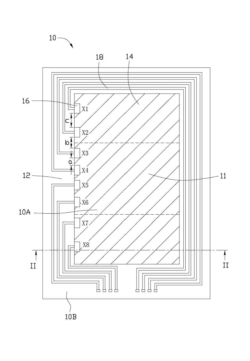
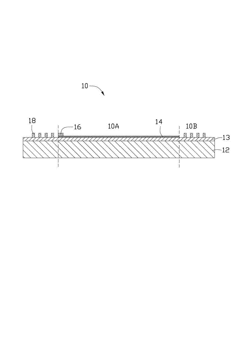
[0016] See figure 1 and figure 2 , the embodiment of the present invention provides a touch screen panel 10 , the touch screen panel 10 includes an insulating substrate 12 , an adhesive layer 13 , a transparent conductive layer 14 , a plurality of sensing electrodes 16 , and a plurality of wires 18 . The plurality of sensing electrodes 16 are arranged at intervals on one side of the transparent conductive layer 14 .
[0017] The touch screen panel 10 defines two areas: a touch area 10A and a wiring area 10B. The touch area 10A is an area where the touch screen panel 10 can be touched to realize a touch function, and the wiring area 10B is an area where a plurality of wires 18 are arranged in the touch screen panel 10 . The wiring area 10B is a small area near the edge of the touch screen panel 10 , which may be located on at least one side of the touch area 10A. The touch area 10A is a relatively large area including the central area of the touch screen panel 10 . The w...
specific Embodiment 2
[0038] See Figure 4 and Figure 5 , the embodiment of the present invention further provides a touch screen panel 20 , the touch screen panel 20 includes an insulating substrate 12 , an adhesive layer 13 , a transparent conductive layer 14 , a plurality of sensing electrodes 16 , and a plurality of wires 18 . The plurality of sensing electrodes 16 are arranged at intervals on opposite sides of the transparent conductive layer 14 , and each sensing electrode 16 is electrically connected to the transparent conductive layer 14 .
[0039] The difference between the first embodiment and the second embodiment is: the sensing electrode 16 is only arranged on one side of the transparent conductive layer 14 in the first embodiment, while the sensing electrode 16 is arranged on the transparent conductive layer 14 in the second embodiment opposite sides. Regarding the rest of the structure and materials of the touch screen panel 20 , the second embodiment is the same as the first embo...
PUM
| Property | Measurement | Unit |
|---|---|---|
| Thickness | aaaaa | aaaaa |
| Thickness | aaaaa | aaaaa |
| Diameter | aaaaa | aaaaa |
Abstract
Description
Claims
Application Information