
Eureka
For R&D, Eureka makes reading and utilizing patents & technical documents easy.
Eureka AIR
Designed for self-driven R&D workflows. Generate viable solutions, solve complex R&D challenges, empower your innovation with AI.

Eureka Materials
Designed for material experts only. Revolutionize your material R&D, from search, analyze, to developing new materials.

TechResearch
Generate reliable direction feasibility study reports for your R&D in just a few steps.

TechSeek
Discover and master advanced knowledge NOW. Basics, ideas, possibilities, all at once.

TechMind
As an expert in R&D Theories, TechMind can generates customized viable solutions instantly.

TechRisk
Analyze your overall solution with one click, know your potential R&D risks in advance.

TechMonitor
Get weekly tech updates, stay abreast of the latest tech innovations and key insights.
Method of manufacturing input device
A manufacturing method and a technology of an input device, which are applied in the input/output process of data processing, instruments, electrical digital data processing, etc., can solve the problem of reduced reliability under high temperature conditions, and the appearance of the height difference of the outer edge of the light-transmitting area. Satisfaction, poor appearance, etc.
- Summary
- Abstract
- Description
- Claims
- Application Information
AI Technical Summary
Problems solved by technology
Method used
Image

Examples
no. 1 approach
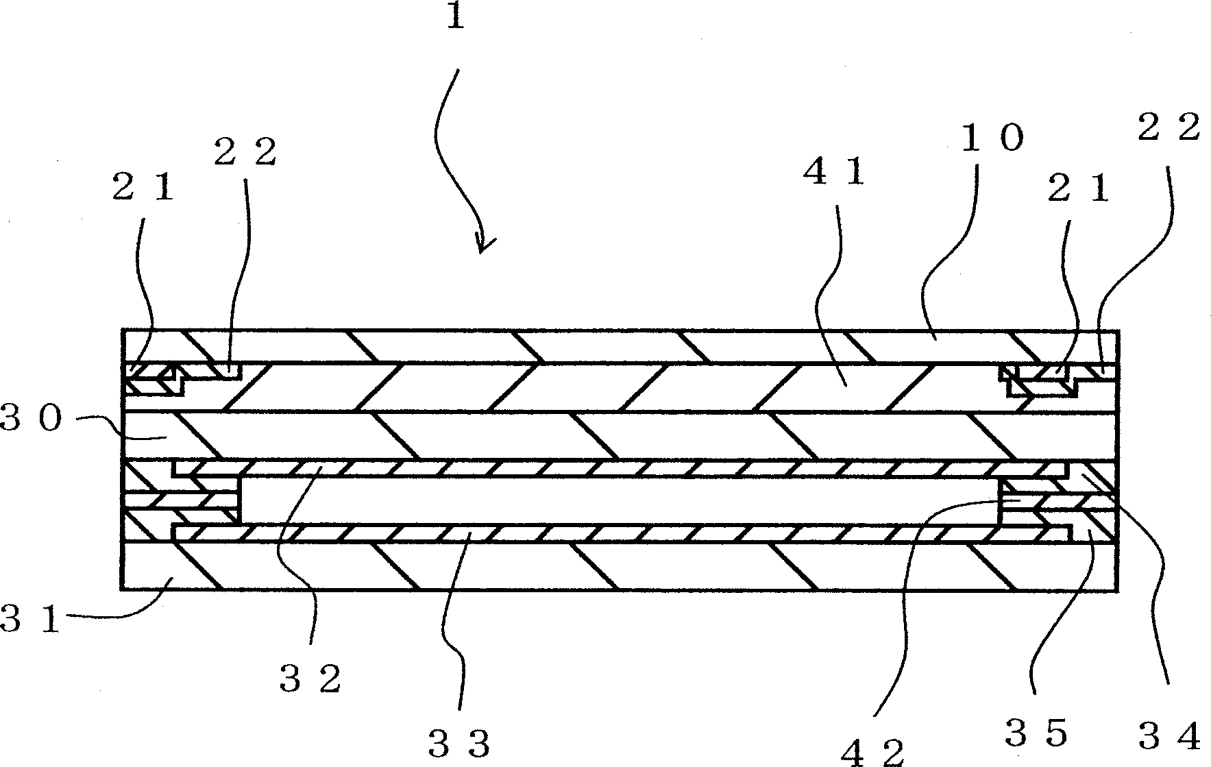
[0062] figure 1 It is a sectional view showing the input device 1 of the first embodiment. like figure 1 As shown, the input device 1 of this embodiment is configured such that the second transparent base material 30 and the third transparent base material 31 are arranged facing each other with a space, and on the upper surface side of the second transparent base material 30 via the first adhesive The junction material 41 is pasted with the first transparent substrate 10 . An upper transparent electrode layer 32 and a lower transparent electrode layer 33 are formed on the opposing surfaces of the second transparent substrate 30 and the third transparent substrate 31 , respectively. Furthermore, on the opposing surfaces of the second transparent base material 30 and the third transparent base material 31 , an upper wiring pattern 34 and a lower wiring pattern 35 are respectively formed on the outer periphery of the transparent electrode layer.
[0063] The first transparen...
no. 2 approach
[0092] Figure 7 to Figure 10 A process diagram showing a manufacturing method of the input device 1 according to the second embodiment. It should be noted that detailed descriptions of the same contents as those in the first embodiment will be omitted.
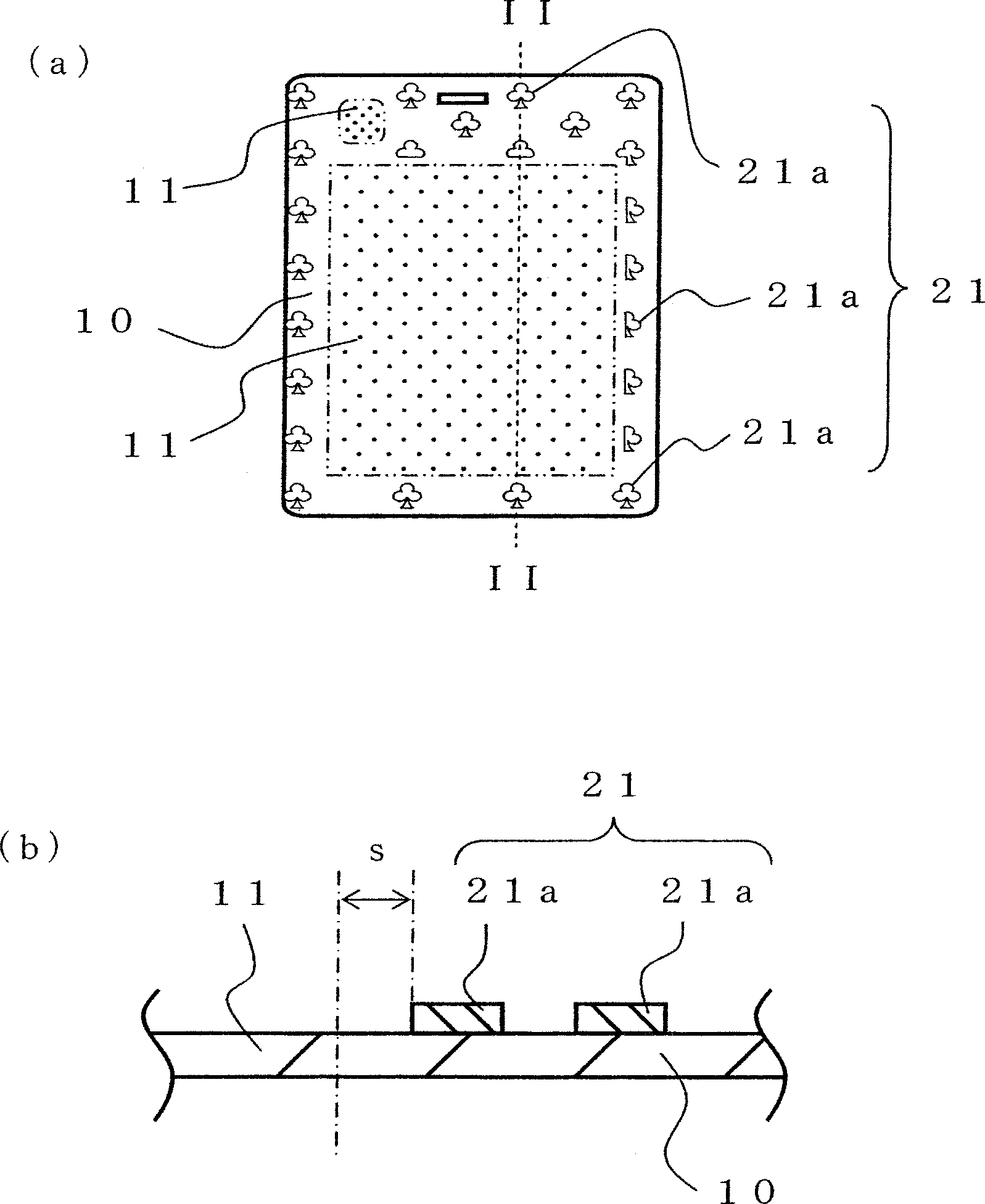
[0093] Figure 7 (a) shows a top view of the first transparent substrate 10, Figure 7 (b) means along Figure 7 (a) A partially enlarged cross-sectional view of the vicinity of the boundary of the light-transmitting region 11 of the first transparent substrate 10 obtained by cutting along line VII-VII. exist Figure 7 (a) and Figure 7 In the step (b), the border layer 24 is formed so as to surround the light-transmitting region 11 of the film-shaped first transparent base material 10 . The border layer 24 is formed by printing methods such as screen printing, inkjet printing, gravure printing, and offset printing. The border layer 24 is provided to make a display image from an external display device such as a liquid...
PUM
 Abstract
Description
Claims
Application Information
 - R&D Engineer
- R&D Manager
- IP Professional
- Industry Leading Data Capabilities
- Powerful AI technology
- Patent DNA Extraction
Browse by: Latest US Patents, China's latest patents, Technical Efficacy Thesaurus, Application Domain, Technology Topic, Popular Technical Reports.
© 2024 PatSnap. All rights reserved.Legal|Privacy policy|Modern Slavery Act Transparency Statement|Sitemap|About US| Contact US: help@patsnap.com