SDRAM (synchronous dynamic random access memory) controller and operating method for same
A controller and address register technology, used in instruments, electrical digital data processing, etc., can solve problems such as read and write rate limitations, CPU does not have burst read and write functions, etc., to improve the efficiency of read and write, and enhance performance.
- Summary
- Abstract
- Description
- Claims
- Application Information
AI Technical Summary
Problems solved by technology
Method used
Image

Examples
Embodiment 1
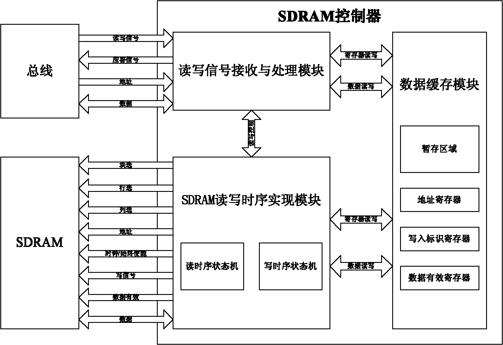
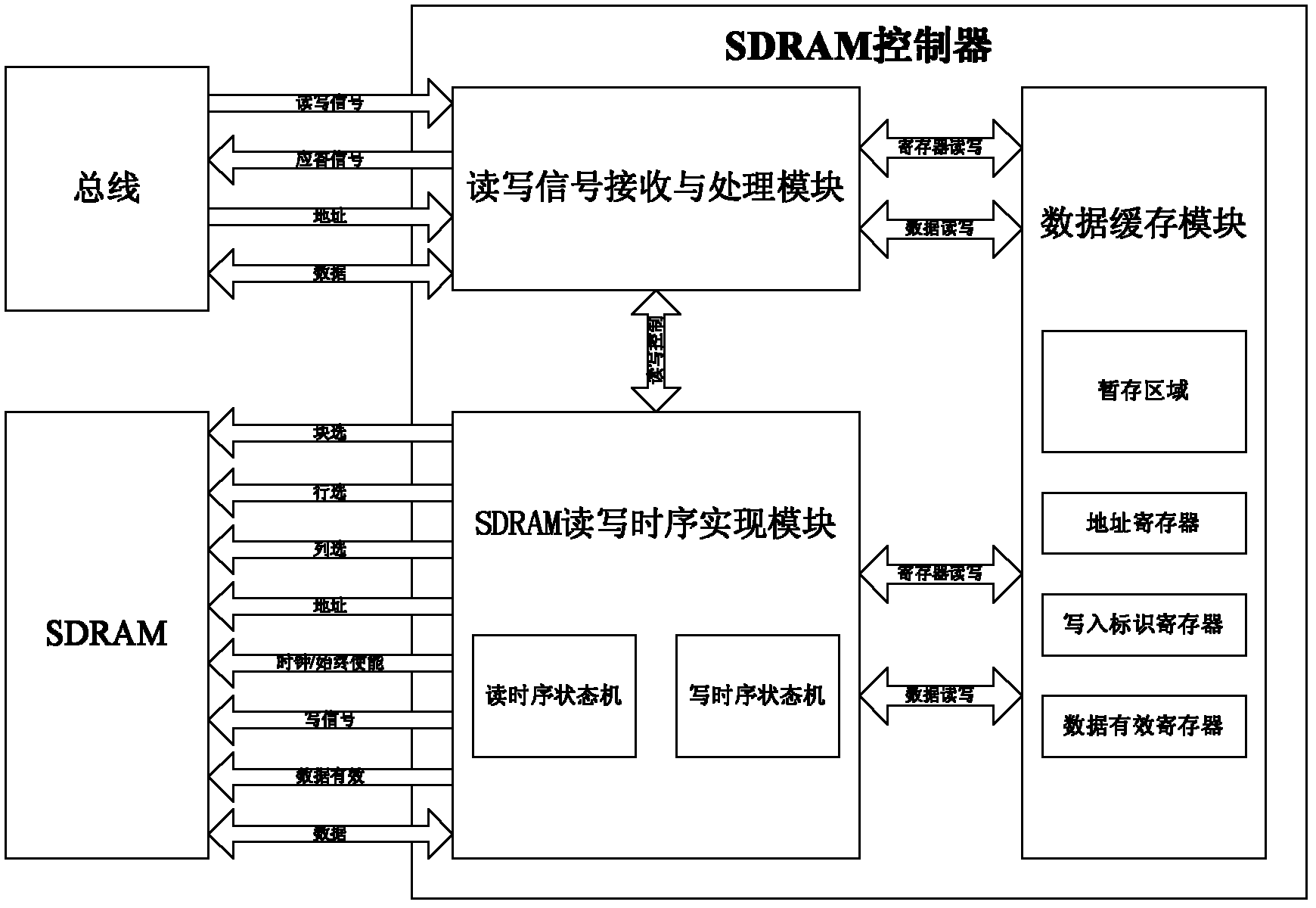
[0035] Such as figure 1 Shown, a kind of SDRAM controller comprises read-write signal receiving and processing module, data cache module and SDRAM read-write sequence realization module; Described SDRAM read-write sequence realization module comprises read sequence state machine and write sequence state machine; Described The data cache module comprises a temporary storage area, an address register, a write-in identification register and a valid data register; the read-write signal receiving and processing module is connected with the external bus, and the SDRAM read-write timing realization module is connected with a random dynamic memory (SDRAM) connected. The read-write signal receiving and processing module is connected to the external bus through data lines, address lines, read-write signal lines and response signal lines; line, block selection line, clock / clock enable line, write signal line and data valid line are connected with the random dynamic memory (SDRAM).
Embodiment 2
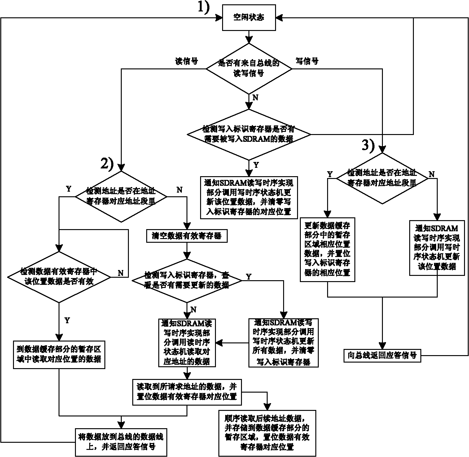
[0037] Such as figure 2 As shown, as described in Embodiment 1, a working method of an SDRAM controller, the method steps are as follows:
[0038] 1) The SDRAM controller is initially in an idle state, and the read and write signal receiving and processing module detects whether it receives a read and write request signal from the bus:
[0039] a. If a read request from the bus is received, proceed to step 2);
[0040] b. If a write request from the bus is received, proceed to step 3);
[0041] c. If no read or write request from the bus is received, then detect whether there is data in the write identification register of the data cache module that needs to be written into SDRAM for updating:
[0042] c1. If there is data to be written into SDRAM, notify the SDRAM read and write sequence implementation module to initiate a write operation, and write the data to be updated to the corresponding address of SDRAM;
[0043]c2. If no data needs to be written into the SDRAM, the...
PUM
 Abstract
Description
Claims
Application Information
 - R&D Engineer
- R&D Manager
- IP Professional
- Industry Leading Data Capabilities
- Powerful AI technology
- Patent DNA Extraction
Browse by: Latest US Patents, China's latest patents, Technical Efficacy Thesaurus, Application Domain, Technology Topic.
© 2024 PatSnap. All rights reserved.Legal|Privacy policy|Modern Slavery Act Transparency Statement|Sitemap