Multi-diffusion manufacturing method for polycrystalline silicon wafer

A technology of multiple diffusion and manufacturing methods, which is applied in the directions of diffusion/doping, final product manufacturing, chemical instruments and methods, etc., and can solve the problems such as the difficulty of distinguishing the colors of the front and back sides

Active Publication Date: 2012-07-04
YINGLI ENERGY CHINA
View PDF5 Cites 10 Cited by
  • Summary
  • Abstract
  • Description
  • Claims
  • Application Information

AI Technical Summary

Problems solved by technology

[0011] The technical problem to be solved by the present invention is to provide a manufacturing method for multiple diffusion of polycrystalline silicon wafers, which can realize the purpose of solving the problem that the color of the front and back sides is not easy to distinguish after the PN junction of multi-wafers is manufactured

Method used


Image

  • Multi-diffusion manufacturing method for polycrystalline silicon wafer
  • Multi-diffusion manufacturing method for polycrystalline silicon wafer
  • Multi-diffusion manufacturing method for polycrystalline silicon wafer

Examples


Embodiment Construction

[0032] The core of the present invention is to provide a manufacturing method of multi-diffusion of multi-chip PN junctions, which can realize the purpose of solving the problem that the color of the front and back sides is not easy to distinguish after multi-chip manufacturing of PN junctions .

[0033] In order to enable those skilled in the art to better understand the technical solutions of the present invention, the present invention will be further described in detail below in conjunction with the accompanying drawings and specific embodiments.

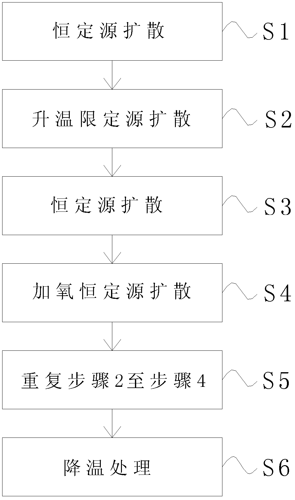
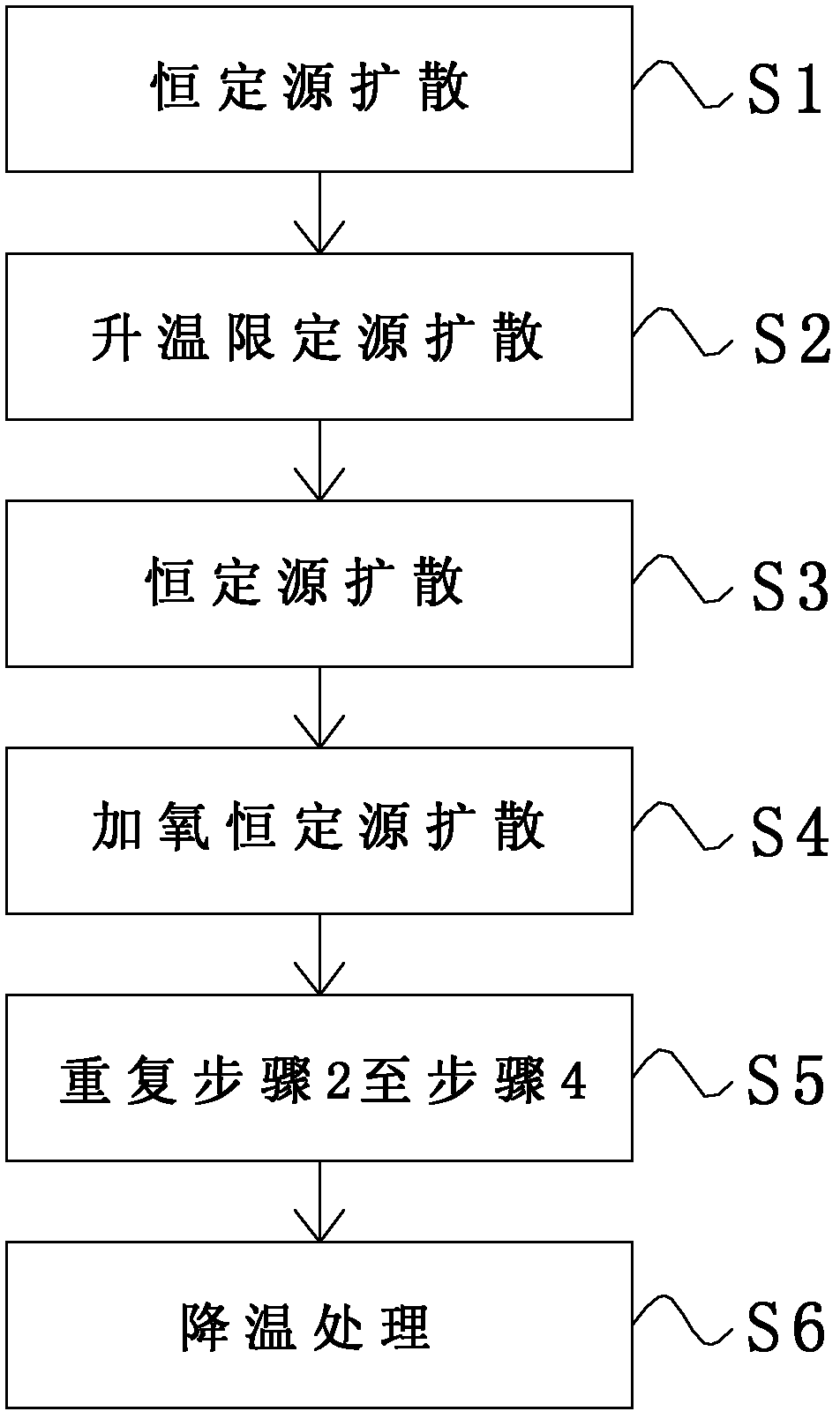
[0034] Please refer to figure 2 , figure 2 It is a flow chart of the multi-diffusion process for PN junctions made of multi-wafers provided by the present invention.

[0035]The invention provides a method for manufacturing multi-diffusion of PN junctions made of multiple wafers, the method comprising: step S1 constant source diffusion, step S2 temperature rise limited source diffusion, step S3 constant source diffusion, ste...


PUM

PropertyMeasurementUnit
electrical resistanceaaaaaaaaaa
thicknessaaaaaaaaaa

Abstract

The invention discloses a multi-diffusion manufacturing method for a PN junction manufactured of a polycrystalline wafer. The multi-diffusion manufacturing method comprises the following steps of: S1, depositing, by constant source diffusion, an impurity source of certain concentration on the surface layer on which a P layer is required to be formed; S2, heating finite source diffusion to perform internal diffusion on a deposited impurity source phase polycrystalline wafer to control junction depth of the PN junction and gradient distribution of an impurity source; S3, depositing, by the constant source diffusion, the impurity source of the certain concentration on the surface layer of the P layer of the polycrystalline wafer again; S4, increasing, by oxygenation constant source diffusion, flux of oxygen under the conditions of unchanged temperature and a continuous flux source, wherein the step aims to increase the surface color of the P layer of the polycrystalline wafer, so that a front face and a back face of the polycrystalline wafer are differentiated during subsequent operation, and the hydrophilicity of the P layer can also be improved by increase in oxygen flux, so that an over large etching edge is reduced; and S5, repeating the step S2 to the step S4. Through the steps, the aim of solving the problem of difficulty in differentiating the colors of the front face and the back face existing after manufacturing of the PN junction of the polycrystalline wafer can be fulfilled.

Description

technical field [0001] The invention relates to the technical field of solar battery modules, in particular to a method for manufacturing polycrystalline silicon wafers with multiple diffusions. Background technique [0002] With the continuous deterioration of the environment and the increasing shortage of energy, strengthening environmental protection and developing clean energy has become a matter of great concern to all countries in the world. As an important photoelectric energy conversion device, the research of solar cells has attracted people's attention. In recent years, with the development and utilization of new technologies, new processes and new structures of solar cells, the photovoltaic industry has developed rapidly. For the polysilicon solar cell industry, reducing the cost of solar cells and improving the conversion efficiency of solar cells have become the two main goals of industry development and competition. From a technical point of view, improving a...

Claims


Application Information

Patent Timeline
Patent Type & Authority Applications(China)
IPC IPC(8): H01L31/18C30B31/06C30B31/16C30B31/18
CPCY02P70/50
Inventor 范志东王静张东升赵学玲吝占胜
Owner YINGLI ENERGY CHINA
Why Eureka
Try Eureka