Supercharge Your Innovation With Domain-Expert AI Agents!

Active element

A technology of active components and sources, which is applied in the direction of electrical components, semiconductor devices, transistors, etc., and can solve the problem of increasing the layout area of ​​components

Active Publication Date: 2014-11-05
AU OPTRONICS CORP
View PDF9 Cites 0 Cited by
  • Summary
  • Abstract
  • Description
  • Claims
  • Application Information

AI Technical Summary

Problems solved by technology

However, increasing channel width tends to result in a substantial increase in component layout area

Method used


Image

  • Active element
  • Active element
  • Active element

Examples


Embodiment Construction

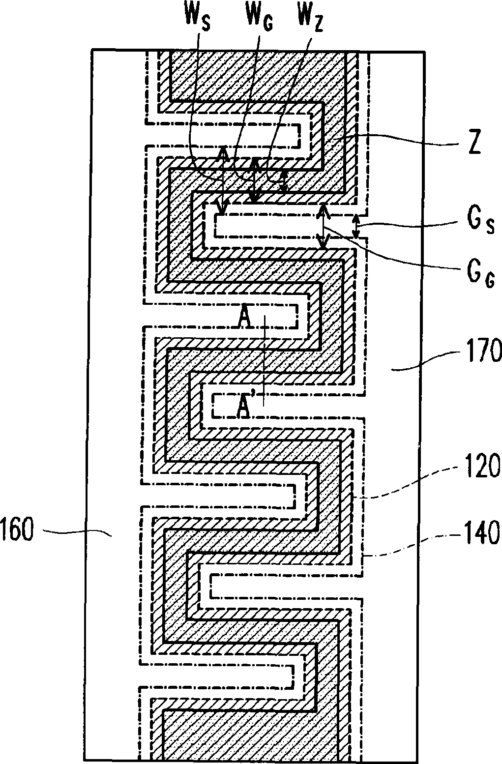
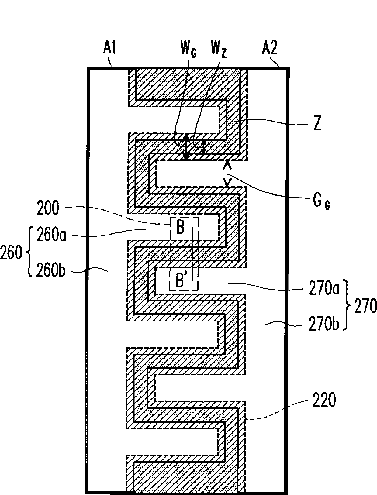
[0050] Figure 2A is a schematic layout diagram of an active element according to an embodiment of the present invention, and Figure 2B for along Figure 2A The schematic cross-section obtained by the section line B-B'. Please refer to Figure 2A and Figure 2B , the active device 200 of this embodiment is suitable to be fabricated on a substrate 210 . The active device 200 includes a gate 220 , a gate insulating layer 230 , an oxide semiconductor layer 240 , an insulating layer 250 , a source 260 and a drain 270 .

[0051] In this embodiment, the gate 220 is disposed on the substrate 210, and the material of the gate 220 is, for example, metal. The gate insulating layer 230 is disposed on the gate 220 , and the material of the gate insulating layer 230 is, for example, silicon oxide, silicon nitride or other suitable dielectric materials. The oxide semiconductor layer 240 is disposed on the gate insulating layer 230 and located above the gate 220 to serve as a channel la...


PUM


Abstract

An active device including a source, a drain, an oxide semiconductor layer, a gate and a gate insulator layer is provided. The source includes first stripe electrodes parallel to each other and a first connection electrode connected thereto. The drain includes second stripe electrodes parallel to each other and a second connection electrode connected thereto, wherein the first stripe electrodes and the second stripe electrodes are parallel to each other, electrically isolated, and alternately arranged, and a zigzag trench is formed therebetween. The gate extends along the zigzag trench. The oxide semiconductor layer is in contact with the source and drain, wherein a contact area among the oxide semiconductor layer and each first stripe electrodes substantially equals to a layout area of each first stripe electrodes and a contact area among each second stripe electrodes substantially equals to a layout area of each second stripe electrodes.

Description

technical field [0001] The invention relates to an active element, in particular to an active element with an oxide semiconductor layer. Background technique [0002] Among many flat-panel displays, Thin Film Transistor Liquid Crystal Display (TFT-LCD) has superior characteristics such as high space utilization efficiency, low power consumption, no radiation and low electromagnetic interference. Therefore, LCD displays are favored by consumers. welcome. The thin film transistor liquid crystal display is mainly composed of an active matrix substrate, a color filter substrate and a liquid crystal layer located between the two substrates. The active array substrate has an active area and a peripheral circuit area. The active array is located in the active area, and the driving circuit is located in the peripheral circuit area. [0003] Taking the driving circuit on the peripheral circuit area as an example, thin film transistors with a high ratio of channel width to channel ...

Claims


Application Information

Patent Timeline
Patent Type & Authority Patents(China)
IPC IPC(8): H01L29/786H01L29/10H01L29/423
CPCH01L29/41733H01L29/42384H01L29/7869
Inventor 邱皓麟林其叡曹书玮林俊男叶柏良曾贤楷
Owner AU OPTRONICS CORP
Features
  • R&D
  • Intellectual Property
  • Life Sciences
  • Materials
  • Tech Scout
  • Unparalleled Data Quality
  • Higher Quality Content
  • 60% Fewer Hallucinations
Learn More