Method, device and system for processing circuit board

A technology of circuit board and circuit layer, which is applied in the direction of printed circuit, printed circuit manufacturing, and electrical connection formation of printed components, etc., which can solve problems such as difficult to determine the position of the alignment target, unrecognizable alignment target, poor alignment accuracy, etc. , to achieve the effect of enhancing the CCD system to identify the alignment target

Inactive Publication Date: 2012-07-11
PEKING UNIV FOUNDER GRP CO LTD
View PDF5 Cites 0 Cited by
  • Summary
  • Abstract
  • Description
  • Claims
  • Application Information

AI Technical Summary

Problems solved by technology

[0003] In the above process, slight oxidation was formed when the circuit layer was withdrawn, which caused the CCD (Charge Coupled Device) system of the subsequent exposure machine to fail to recognize the target surface due to the oxidation of the target surface when the copper pillar layer was produced. Position target, causing poor alignment accuracy
Moreover, since the texture of the conductive layer and the target is copper, and the texture of the background conductive layer is also copper, it is difficult to determine the position of the alignment target

Method used


Image

  • Method, device and system for processing circuit board
  • Method, device and system for processing circuit board
  • Method, device and system for processing circuit board

Examples


Embodiment Construction

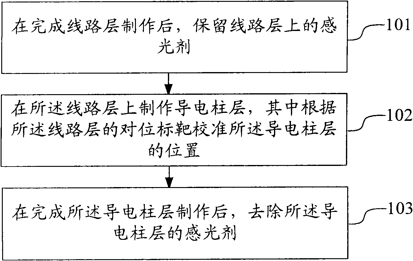
[0028] The invention provides a method for processing circuit boards, characterized in that the method comprises:

[0029] After completing the production of the circuit layer, keep the photosensitive agent on the circuit layer;

[0030] making a conductive column layer on the circuit layer, wherein the position of the conductive column layer is calibrated according to the alignment target of the circuit layer;

[0031] After the fabrication of the conductive column layer is completed, the photosensitive agent of the conductive column layer is removed.

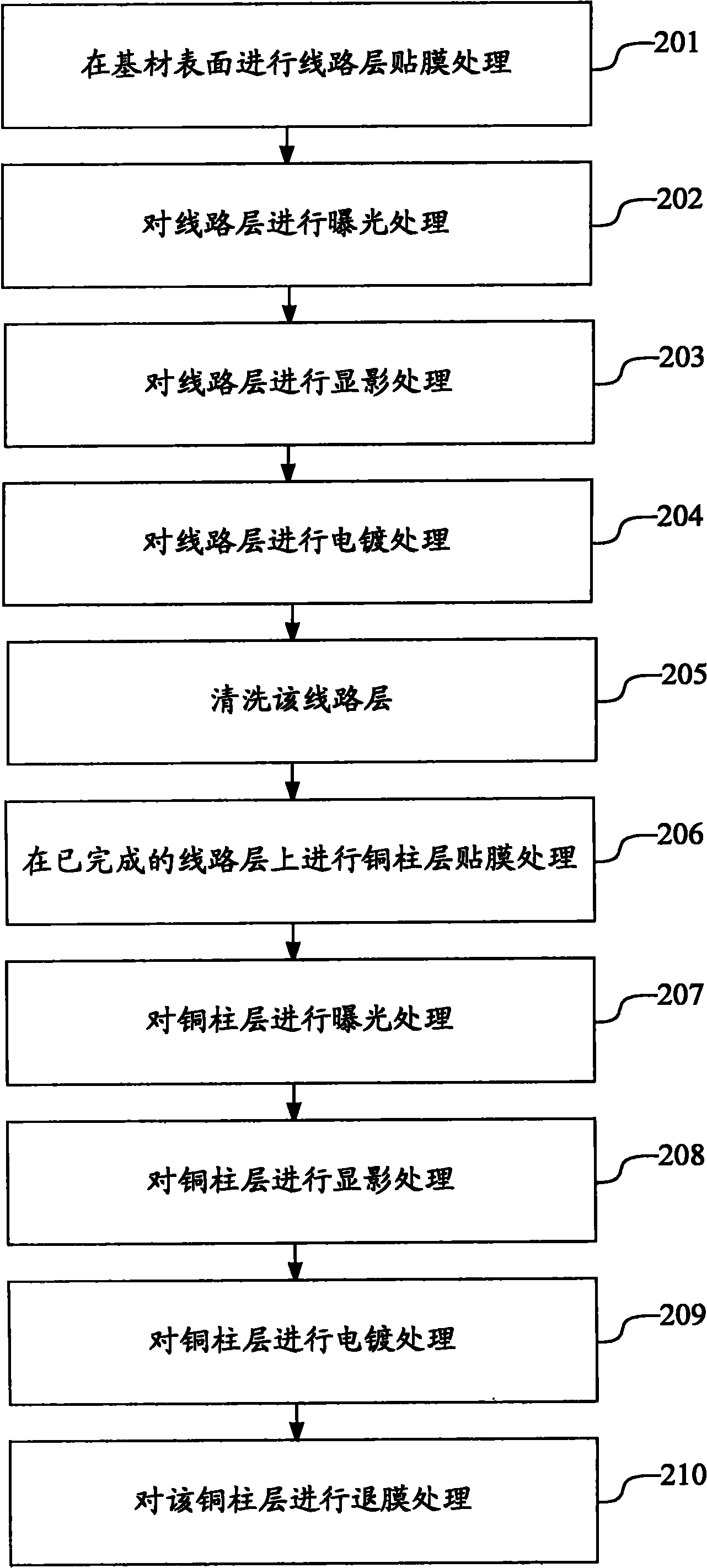
[0032] Preferably, in each embodiment of the present invention, after the circuit layer is fabricated, the circuit layer is cleaned, preferably with an acidic solution.

[0033] Preferably, in each embodiment of the present invention, the alignment target is determined when manufacturing the circuit layer.

[0034] Preferably, in each embodiment of the present invention, when making the circuit layer or the conductive column...


PUM


Abstract

The invention relates to the circuit board technology, particularly to a method, device and system for processing a circuit board. The method comprises the following steps: preserving sensitizer on the circuit layer after a circuit layer is made; making a conductive pole layer on the circuit layer; wherein, the position of the conductive pole layer is corrected according to a position correction target of the circuit layer; and removing the sensitizer of the conductive pole layer after the conductive pole layer is made. By adopting the method, device and system for processing the circuit board, disclosed by the embodiment of the invention, film-removing process is carried out after the circuit layer and the copper pole layer are made, thereby preventing oxidization in film removing from affecting the position correction in the making process of the copper pole layer. In addition, by cleaning the circuit layer after the circuit layer is made, copper on the surface of the circuit layer is brighter, thereby enhancing identification of the copper pole layer during position correction.

Description

technical field [0001] The invention relates to circuit board technology, in particular to a method, device and system for processing circuit boards. Background technique [0002] In the field of circuit board manufacturing, technologies such as through holes, blind holes, buried holes, copper paste (or silver paste, etc.) plug holes or copper pillars are used to interconnect adjacent circuit layers, and the interconnection layer containing copper pillars is produced. At the same time, the basic process is to transfer the pattern of the circuit layer on the conductive layer-electroplating of the circuit layer-removing the film of the circuit layer, and then transfer the pattern of the copper pillar layer on the circuit layer-electroplating of the copper pillar layer-removing the film of the copper pillar layer. The circuit board is cleaned. [0003] In the above process, slight oxidation was formed when the circuit layer was withdrawn, which caused the CCD (Charge Coupled D...

Claims


Application Information

Patent Timeline
Patent Type & Authority Applications(China)
IPC IPC(8): H05K3/00H05K3/40
Inventor 苏新虹朱兴华
Owner PEKING UNIV FOUNDER GRP CO LTD
Why Eureka
Try Eureka