Ball attachment device, solder ball picking method and solder ball mounting method

A technology of solder balls and ball planting, which is applied in the fields of electrical components, semiconductor/solid-state device manufacturing, circuits, etc., can solve the problem of uncontrollable number of solder balls, prevent the loss of solder balls, prevent waste, and improve reliability and efficiency Effect

Active Publication Date: 2014-07-09
SAMSUNG SEMICON CHINA RES & DEV +1
View PDF4 Cites 1 Cited by
  • Summary
  • Abstract
  • Description
  • Claims
  • Application Information

AI Technical Summary

Problems solved by technology

The solder balls are attracted to each other due to the static electricity carried, which causes, for example, the solder balls in the air to be attracted to the solder balls that have been sucked by the vacuum nozzle due to electrostatic attraction, so that the number of solder balls sucked by the vacuum nozzle cannot be controlled

Method used


Image

  • Ball attachment device, solder ball picking method and solder ball mounting method
  • Ball attachment device, solder ball picking method and solder ball mounting method
  • Ball attachment device, solder ball picking method and solder ball mounting method

Examples


Embodiment Construction

[0025] Hereinafter, embodiments will be described in detail with reference to the accompanying drawings. Embodiments may, however, be embodied in many different forms and should not be limited to the examples set forth herein. Rather, these examples are provided so that this disclosure will be thorough and complete, and will fully convey the scope of the embodiments to those skilled in the art. In the drawings, the size and relative sizes of layers and regions are exaggerated for clarity. In the drawings, the same reference numerals denote the same elements throughout.

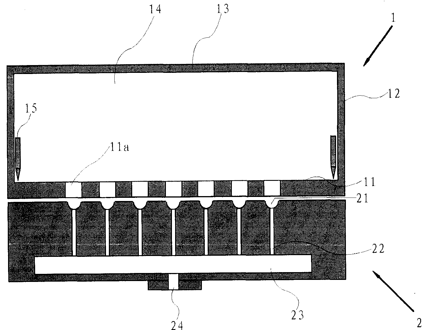
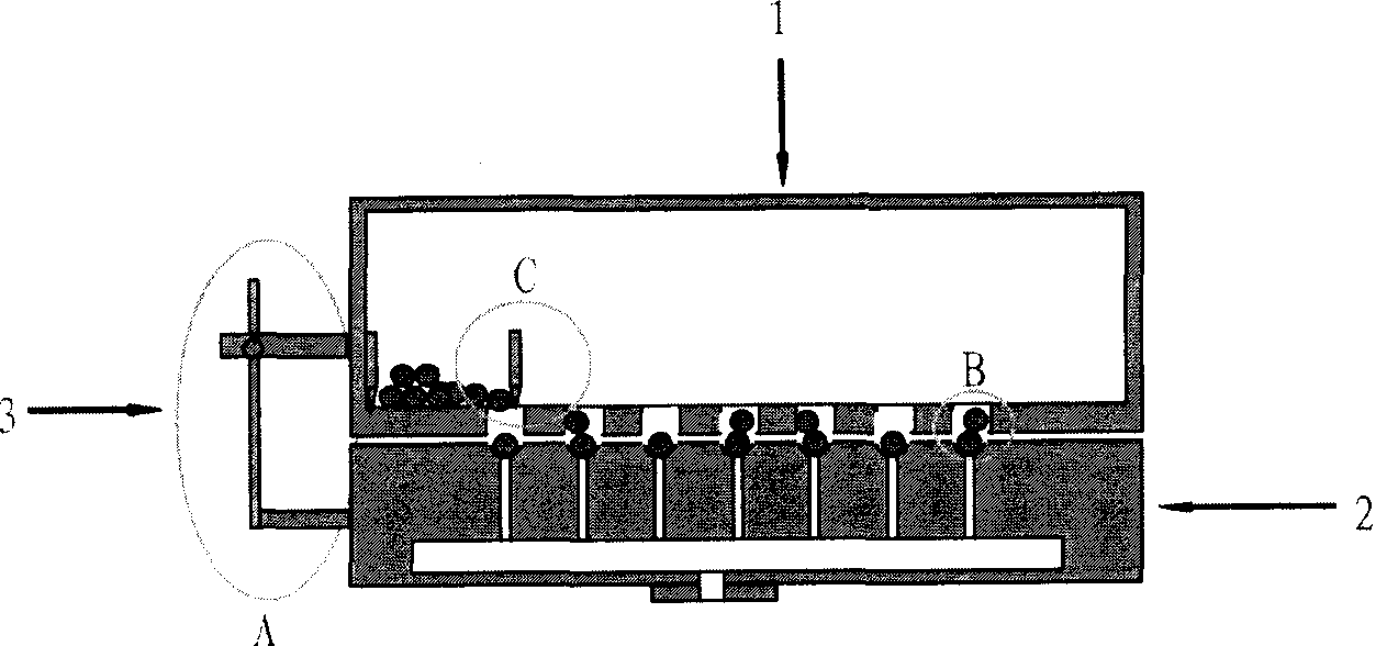
[0026] figure 1 is a sectional view showing a ball planting device according to an embodiment of the present invention. Such as figure 1 As shown in , the ball planting device according to the embodiment of the present invention may include a printing chamber 1 and a vacuum picker 2 .

[0027] The printing chamber 1 comprises a grid template 11 , side walls 12 , a top wall 13 and a doctor blade 15 . The ...


PUM


Abstract

The invention discloses a ball planting device, a solder ball picking method and a solder ball installation method. The ball planting device includes: a printing room, including a grid template, a side wall, a top wall and at least two scrapers, the grid template, the side wall and the top wall are combined to form a loading space, and multiple grid holes, the arrangement pattern of the plurality of grid holes corresponds to the pattern of solder ball mounting positions of components to be mounted with solder balls; a vacuum picker, located below the printing chamber, and includes a plurality of suction nozzles, said At least some of the plurality of suction nozzles are respectively aligned with the plurality of grid holes, wherein the solder balls are loaded in the loading space and pushed through the grid template by moving the scraper so that the solder balls fall into the grid hole and sucked up by the suction nozzle. By adopting the printing method of moving the scraper so that the solder balls fall into the grid holes and are picked up by the suction nozzle, the loss of solder balls can be reduced or prevented, and the reliability and efficiency of the ball planting process can be improved.

Description

technical field [0001] The invention relates to the field of chip packaging, and more specifically, the invention relates to a ball planting device, a method for picking up solder balls, and a method for installing solder balls. Background technique [0002] A ball grid array (BGA) package uses solder balls instead of pins in conventional chip packages to electrically connect the chip to external circuitry. Therefore, compared with other chip packages, the BGA package has the advantages of simple manufacturing process, large number of pins (solder balls) per unit area, high electrical connection reliability, and low manufacturing cost. A traditional process for manufacturing a BGA package (or other components requiring solder balls) includes a ball placement process, that is, picking up solder balls and mounting the picked solder balls to the solder ball mounting positions of the BGA package. [0003] An apparatus for the balling process is disclosed in US Patent Applicatio...

Claims


Application Information

Patent Timeline
Patent Type & Authority Patents(China)
IPC IPC(8): H01L21/60
Inventor 谢晓强
Owner SAMSUNG SEMICON CHINA RES & DEV
Why Eureka
Try Eureka