Check patentability & draft patents in minutes with Patsnap Eureka AI!

Pixel structure and display panel

A pixel structure and display area technology, applied in nonlinear optics, instruments, optics, etc., can solve the problems of decreased aperture ratio, poor light transmittance, complicated production, etc.

Active Publication Date: 2015-02-18
WINTEK CHINA TECH LTD +1
View PDF6 Cites 0 Cited by
  • Summary
  • Abstract
  • Description
  • Claims
  • Application Information

AI Technical Summary

Problems solved by technology

However, the transflective semi-reflective liquid crystal display panel with double-cavity spacing is usually more complicated to manufacture, and each pixel unit often has the problem of poor light transmittance between the transmissive area and the reflective area, resulting in a large aperture ratio. (aperture ratio) drop

Method used


Image

  • Pixel structure and display panel
  • Pixel structure and display panel
  • Pixel structure and display panel

Examples


Embodiment Construction

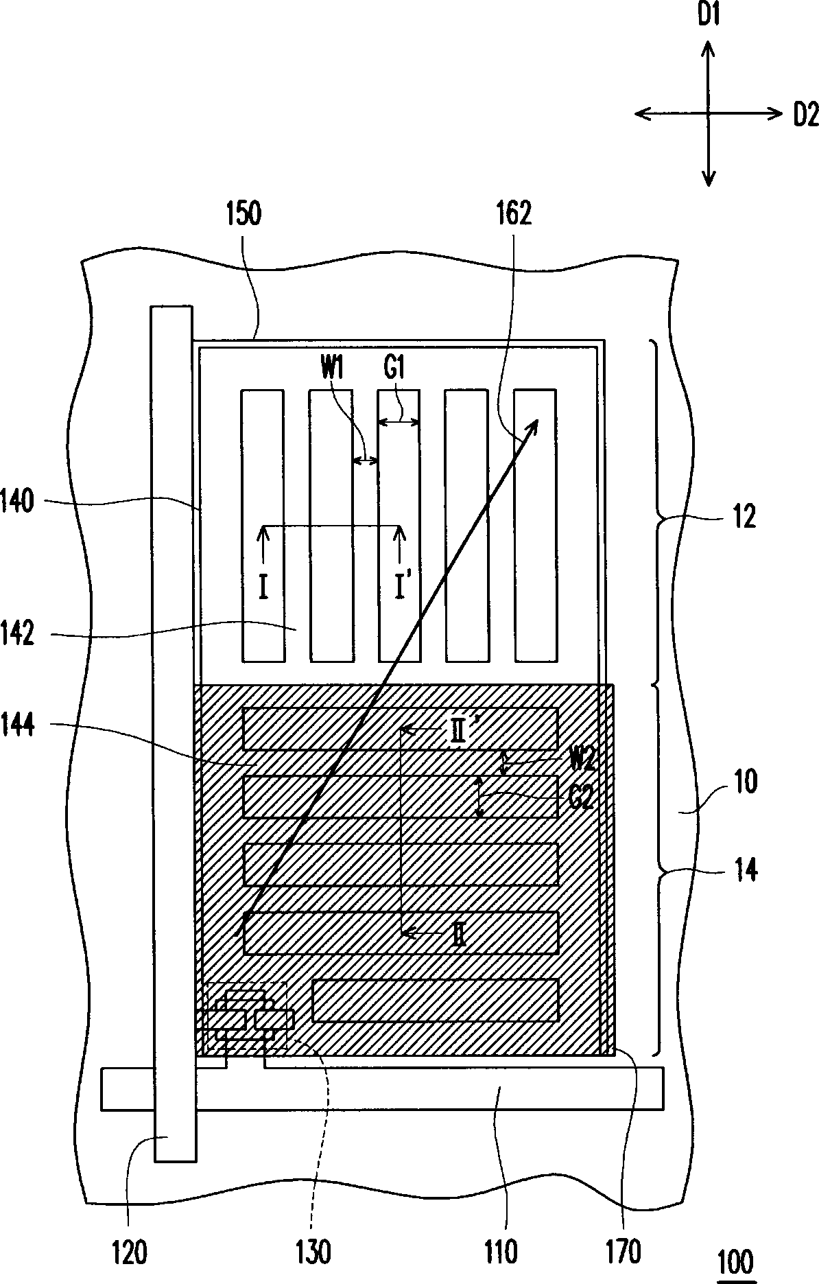
[0040] Figure 1A is the pixel structure of the first embodiment of the present invention, and figure 2 for Figure 1A The cross-sectional view of the pixel structure along the line I-I' and the line II-II'. Please also refer to Figure 1A and figure 2 , the pixel structure 100 is disposed on a substrate 10 . The substrate 10 has a transmissive display area 12 and a reflective display area 14 . The pixel structure 100 includes a scan line 110 , a data line 120 , an active element 130 , a first electrode 140 , a second electrode 150 and an alignment layer 160 . The data line 120 intersects the scan line 110 . The active element 130 is electrically connected to the scan line 110 and the data line 120 . One of the first electrode 140 and the second electrode 150 is electrically connected to the active device 130 , and the other is connected to a common potential. The alignment layer 160 covers the first electrode 140 and the second electrode 150 , and an alignment directio...


PUM


Abstract

The invention provides a pixel structure and a display panel. The pixel structure is configured onto a substrate which is equipped with a first penetration display zone and a reflection display zone. The pixel structure comprises a scanning line, a data line, an active element, a first electrode, a second electrode and an orientation layer. The first electrode is provided with a plurality of first strip-shaped parts which are arranged in the penetration display zone and a plurality of second strip-shaped parts which are arranged in the reflection display zone. Each first strip-shaped part extends along a first direction, and each second strip-shaped part extends along a second direction. The first direction and the second direction are substantially orthogonal to each other. One of the first and second electrodes is electrically connected to the active element, and the other one of the first and second electrodes is connected with a sharing potential. The orientation layer covers the first and second electrodes. One orientation direction of the orientation layer is intersected with the second direction to form an angle of 45 to 85 DEG.

Description

technical field [0001] The present invention relates to a pixel structure and a display panel, in particular to a semi-transmissive-semi-reflective pixel structure and a display panel. Background technique [0002] In recent years, due to the rise of liquid crystal display technology, thin film transistor liquid crystal display (TFT-LCD), which has the advantages of high image quality, light weight, low power consumption and low radiation, has gradually replaced cathode ray tubes and become the mainstream of the display market. If the liquid crystal display is classified according to the utilization method of the light source, it can be roughly classified into two types: transmissive type and reflective type. The transmissive liquid crystal display mainly uses a back light as its display light source, while the reflective liquid crystal display uses a front light source or an external light source as its display light source. [0003] However, with the diversification of ap...

Claims


Application Information

Patent Timeline
IPC IPC(8): G02F1/1362G02F1/1368G02F1/1337
Inventor 林宗贤
Owner WINTEK CHINA TECH LTD
Features
  • R&D
  • Intellectual Property
  • Life Sciences
  • Materials
  • Tech Scout
  • Unparalleled Data Quality
  • Higher Quality Content
  • 60% Fewer Hallucinations
Learn More