

Semiconductor device and memory protection method
A semiconductor and memory technology, applied in memory systems, instruments, preventing unauthorized use of memory, etc., can solve the problem of not distinguishing between main storage devices and auxiliary storage devices, and achieve the effect of protecting information
- Summary
- Abstract
- Description
- Claims
- Application Information
AI Technical Summary
Problems solved by technology
Method used
Image

Examples
no. 1 example
[0030] A semiconductor device and a memory protection method will be described below according to a first embodiment.
[0031] 1. Setup of Semiconductor Devices
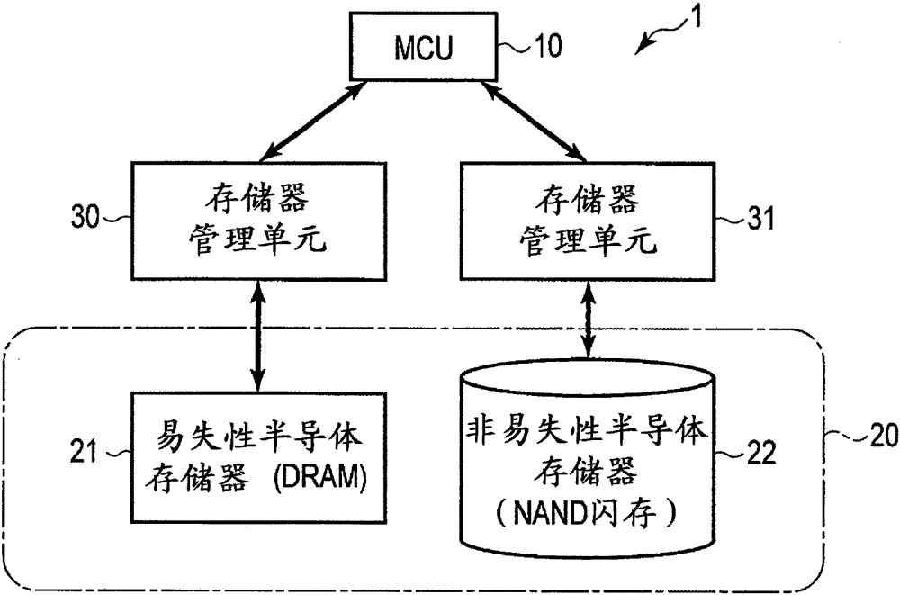
[0032] figure 1 is a block diagram of the semiconductor device according to this embodiment. Such as figure 1 As shown, the semiconductor device 1 includes a processor (MCU: Micro Control Unit) 10 , a memory device 20 , and MMUs (Memory Management Units) 30 and 31 .
[0033] The MCU 10 executes various types of processing using data held in the memory device 20 .
[0034] The storage device 20 includes a volatile semiconductor memory (eg, DRAM in this example) 21 and a nonvolatile semiconductor memory (eg, NAND flash memory in this example) 22 . The DRAM 21 is used as a cache memory of the NAND flash memory 22 . The storage device 20 holds various programs and data such as an OS (Operating System) and applications. DRAM 21 and NAND flash memory 22 are managed by single-level storage technology. Thus, the stora...
no. 2 example
[0106] A semiconductor device and a memory protection method according to a second embodiment are described below. The example at this time relates to the method of allowing worksets to refer to and add new data in the first embodiment. Since other configurations and operations are the same as in the first embodiment, description thereof will not be repeated.
[0107] 1. Data reference
[0108] First, the new data referencing method is described. Figure 15 It is a conceptual diagram of the virtual address space when viewed from workset WS1.
[0109] Such as Figure 15 As shown, the work set WS1 is a set of code CD1 and data D1 as described in the first embodiment. In pages PG45 to PG47 starting at virtual address ADD5, it is assumed that the memory device 20 stores data D3 not included in the work set WS1. The following assumes a situation in which workset WS1 requires data D3.
[0110] Figure 16 A flowchart showing the operation sequence of the semiconductor device 1...
no. 3 example
[0130] A semiconductor device and a memory protection method according to a third embodiment will be described below. This embodiment manages information in the storage device 20 using files and directories of the FAT (File Allocation Table) file system as in the first or second embodiment. Since other configurations and operations are the same as those in the first or second embodiment, description thereof will not be repeated.
[0131] 1. Using directory structure management
[0132] Figure 19 is a conceptual diagram of the virtual address space of the storage device 20 according to this embodiment. Assume that code CD1 is stored in pages PG0 to PG2, code CD2 is stored in pages PG10 to PG12, and data D1 is stored in pages PG30 to PG40, as Figure 19 shown.
[0133] In this case, the MCU 10 manages the code CD1 as a file AAA, manages the code CD2 as a file BBB, and manages the data D1 as two files CCC and DDD. In addition, MCU10 manages these files in a tree structure, ...
PUM
 Abstract
Description
Claims
Application Information