Silicon-on-insulator (SOI)/metal oxide semiconductor (MOS) device structure for connecting negative voltage on backgate through negative charge pump and manufacturing method

A technology of MOS devices and negative charge pumps, applied in semiconductor/solid-state device manufacturing, electric solid-state devices, electrical components, etc., can solve problems affecting device performance, simplify process steps, improve back gate threshold voltage drift effect, eliminate effect of influence

Active Publication Date: 2012-10-03
58TH RES INST OF CETC
View PDF5 Cites 2 Cited by
  • Summary
  • Abstract
  • Description
  • Claims
  • Application Information

AI Technical Summary

Problems solved by technology

Such positive charge accumulation will cause a source/drain channel to be formed on the back of the device, which is not controlled by the front g

Method used


Image

  • Silicon-on-insulator (SOI)/metal oxide semiconductor (MOS) device structure for connecting negative voltage on backgate through negative charge pump and manufacturing method
  • Silicon-on-insulator (SOI)/metal oxide semiconductor (MOS) device structure for connecting negative voltage on backgate through negative charge pump and manufacturing method
  • Silicon-on-insulator (SOI)/metal oxide semiconductor (MOS) device structure for connecting negative voltage on backgate through negative charge pump and manufacturing method

Examples


Embodiment Construction

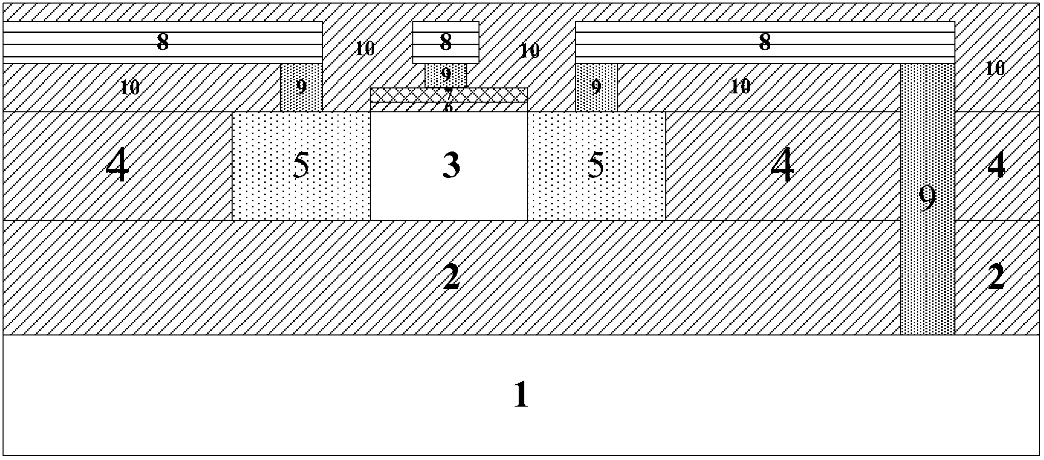
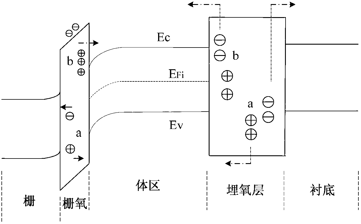
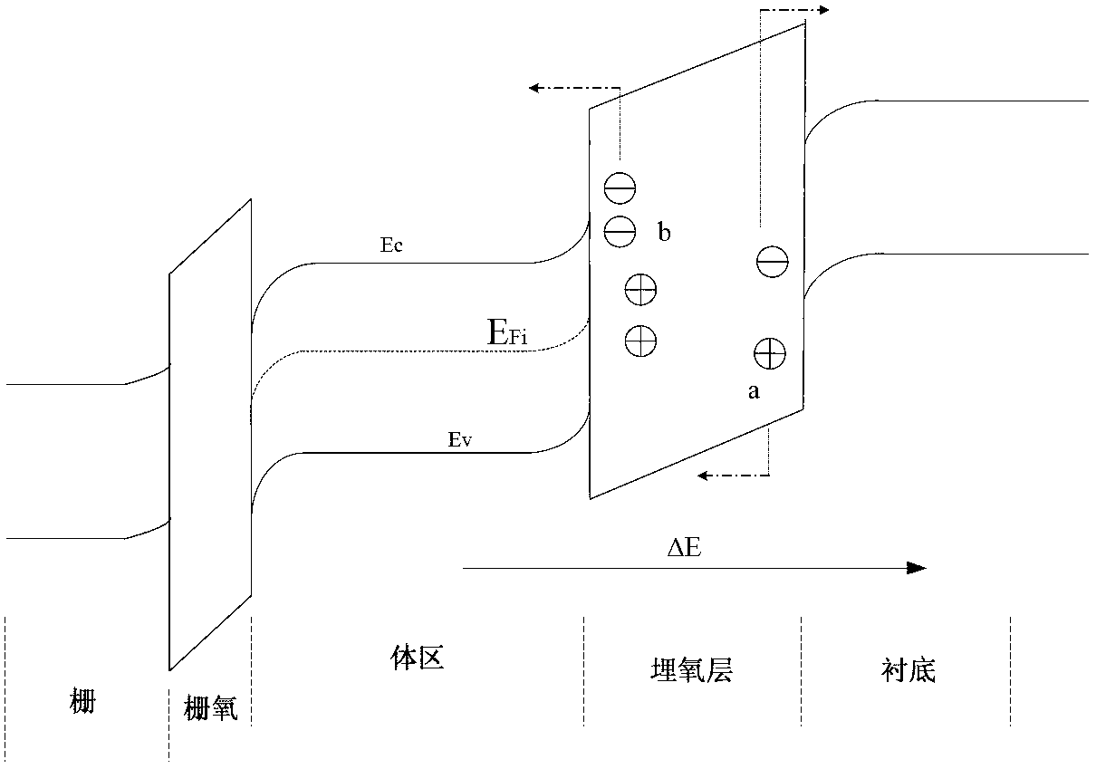
[0018] The present invention will be further described below in conjunction with drawings and embodiments. The invention relates to the SOI / MOS device structure and manufacturing method with negative voltage connected to the back gate. By opening holes from the front side of the silicon film of the SOI / MOS device, the contact hole passes through the buried oxide layer, and the substrate is connected to the surface of the SOI / MOS device. Negative charge pump to improve the back gate effect of partially depleted SOI / MOS devices under radiation conditions. The basic principle of this design is: use the back substrate to connect negative voltage to change the electric field distribution in the buried oxide layer of SOI / MOS devices, so as to affect the accumulation of positive charges at the back gate interface under radiation conditions, so as to eliminate the impact caused by the total radiation dose. The influence of back gate effect on device performance.

[0019] Such as fig...


PUM


Abstract

The invention relates to a silicon-on-insulator (SOI)/metal oxide semiconductor (MOS) device structure for connecting negative voltage on back gate through a negative charge pump and a manufacturing method. The manufacturing method is characterized in that the front surface of an SOI/MOS device silicon film is perforated, a contact hole runs through a buried oxide layer, and a substrate is connected to the negative charge pump on the surface of the SOI/MOS device, so that the back gate effect of the partially-use-up SOI/MOS device under the radiation condition can be improved. The basic principle for designing the SOI/MOS device structure is that a back substrate is connected with the negative voltage, so that the distribution of an electric field inside the SOI/MOS device buried oxide layer is changed so as to influence the accumulation of positive charges on the interface of the back gate under the radiation condition, and the influence of the back gate effect caused by the radiation total dose on the performance of the device can be eliminated. Due to the adoption of the method, not only is the problem that the voltage of the back substrate of the SOI/MOS device is uncertain solved, but also the additional technique reinforcement for the back gate is not required in the manufacturing process of the device, and the process steps can be simplified. The back gate is connected with the negative voltage, so that the total dose resistance of the partially-use-up SOI/MOS circuit can be improved, and the performance of other circuits on the surface is not influenced.

Description

technical field [0001] The invention relates to the anti-radiation strengthening technology of SOI / MOS devices, in particular to a SOI / MOS device structure and a manufacturing method in which a negative voltage is connected to a back gate through a negative charge pump. Background technique [0002] SOI technology refers to the material preparation technology of forming a single crystal semiconductor silicon thin film layer with a certain thickness on the insulating layer and the process technology of manufacturing semiconductor devices on the thin film layer. This technology can achieve complete dielectric isolation. Compared with bulk silicon devices isolated by P-N junctions, it has the advantages of no latch, high speed, low power consumption, high integration, high temperature resistance, and radiation resistance. [0003] According to the thickness of SOI silicon film, SOI devices can be divided into thick film devices and thin film devices. For thick-film SOI devices...

Claims


Application Information

Patent Timeline
IPC IPC(8): H01L27/12H01L21/762H01L21/84
Inventor 周昕杰罗静陈嘉鹏王栋洪根深
Owner 58TH RES INST OF CETC
Why Eureka
Try Eureka