Substrate stacking structure
A stacking structure and substrate technology, applied in the field of stacking structures, can solve problems such as broken metal wires, difficulty in reducing the thickness of the stacking structure, and difficult independent testing of chips on different platforms, etc., to achieve the effect of reducing the overall thickness
- Summary
- Abstract
- Description
- Claims
- Application Information
AI Technical Summary
Problems solved by technology
Method used
Image
Examples
Embodiment Construction
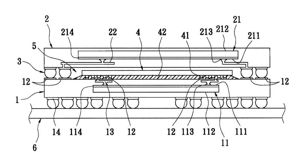
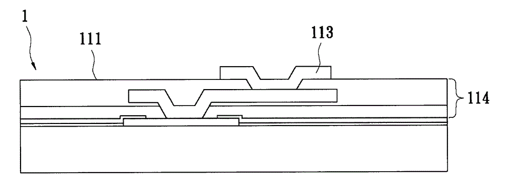
[0056] see figure 2 with image 3 , which is a preferred embodiment of the present invention, where figure 2 It is a schematic diagram of the present invention, image 3 for figure 2 magnified schematic diagram.
[0057] refer to figure 2 , which is a substrate stack structure, including a first substrate (substrate) 1 embedded with a first chip (die) 11, a second substrate (substrate) 2 embedded with a second chip (die) 12, several connections to the above-mentioned The soldering part 3 of the first substrate 1 and the second substrate 2 , and a third die 4 disposed between the first substrate 1 and the second substrate 2 . Wherein, the above-mentioned soldering part 3 conducts the first substrate 1 and the second substrate 2 , and the first substrate 1 , the second substrate 2 and the soldering part 3 surround and form an accommodating space 5 . The third chip 4 is disposed in the accommodating space 5 and bonded to one end surface of the first substrate 1 , and th...
PUM
 Abstract
Description
Claims
Application Information


