Method for recording chip use state information, imaging box chip and imaging box

A state information, imaging box technology, applied in the direction of electrical recording, data processing input/output process, printing, etc., can solve the problem of not recording the use status of the chip, unable to analyze the chip failure, unusable imaging box, etc.

Active Publication Date: 2012-11-07
APEX MICROELECTRONICS CO LTD
View PDF8 Cites 22 Cited by
  • Summary
  • Abstract
  • Description
  • Claims
  • Application Information

AI Technical Summary

Problems solved by technology

However, the above state parameters can only reflect the use state of the imaging box, and do not record the use state of the chip itself
If there is a problem w

Method used


Image

  • Method for recording chip use state information, imaging box chip and imaging box
  • Method for recording chip use state information, imaging box chip and imaging box
  • Method for recording chip use state information, imaging box chip and imaging box

Examples


Embodiment Construction

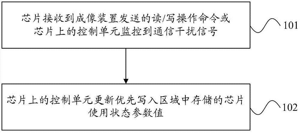
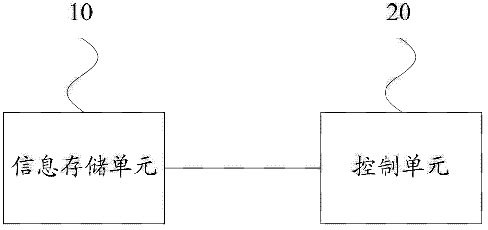
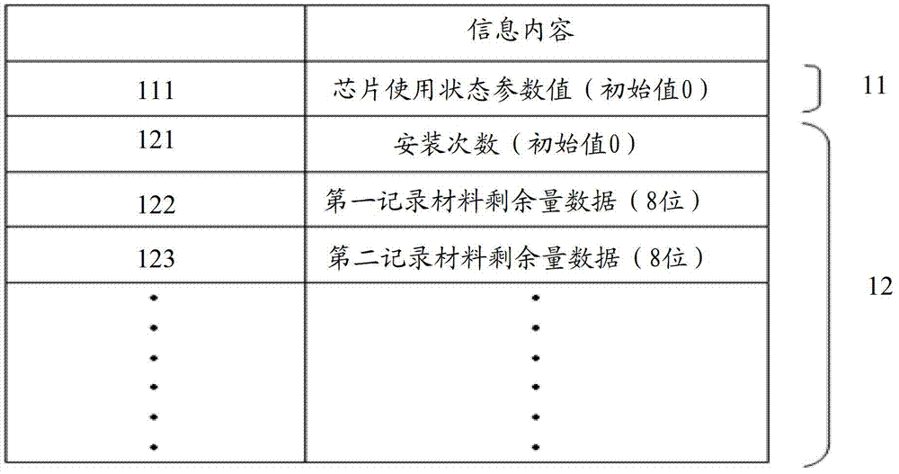
[0018] figure 1 It is a flowchart of a method for recording chip usage status information in the first embodiment of the present invention. The chip includes a substrate and an information storage unit and a control unit arranged on the substrate. The information storage unit includes a priority writing area and a regular reading and writing area, such as figure 1 As shown, the method includes:

[0019] Step 101, the chip receives a read / write operation command sent by the imaging device or the control unit on the chip monitors a communication interference signal;

[0020] Step 102 , the control unit on the chip updates the chip usage state parameter value stored in the priority writing area; the above chip usage state parameter value is used for fault analysis on the chip.

[0021] After the above step 102 is executed, the control unit on the chip can also update the data recorded in each storage area in the normal read / write area.

[0022] The imaging box is a component on...


PUM


Abstract

The invention provides a method for recording the chip use state information, an imaging box chip and an imaging box. The imaging box chip comprises a base plate, an information memory unit and a control unit, wherein the information memory unit and the control unit are arranged on the base plate, and the information memory unit comprises a prior write-in region and an ordinary read-white region. The method for recording the use state information comprises the following steps that when the chip receives read/write operation commands sent by an imaging device or a control unit arranged on the chip monitors communication interference signals, the control unit arranged on the chip updates the chip use state parameter values stored in the prior write-in region, and the chip use state parameter values are used for carrying out fault analysis on the chip. The imaging box comprises the imaging box chip. The recorded chip use state parameter values can reflect the use state information of the chip per se, and powerful data is provided for discovering and solving the communication problem between the chip and the imaging device.

Description

technical field [0001] The invention relates to imaging technology, in particular to a method for recording chip use state information, a chip of an imaging box and the imaging box. Background technique [0002] With the development of imaging technology, imaging devices such as copiers, printers, facsimile machines, and word processors have been widely used. Imaging devices are equipped with consumables such as imaging boxes that are convenient for users to replace. The imaging boxes are usually equipped with chips, which record the types of recording materials stored in the imaging box, the manufacturing date of the imaging box, the number of imaging pages, and the remaining recording materials. quantity and other information. During the use of the imaging box, the imaging device needs to continuously update the data in the chip on the imaging box, so that the latest state of the imaging box is always recorded in the chip. Therefore, the chip on the imaging box is partic...

Claims


Application Information

Patent Timeline
IPC IPC(8): B41J2/175G03G21/18B41J29/38
CPCB41J2/175B41J2/17546G06F11/0733G06F11/3476G06F11/3013G06F11/0745G06F11/0787G06F3/121G06F3/1235
Inventor 刘卫臣
Owner APEX MICROELECTRONICS CO LTD
Why Eureka
Try Eureka