Check patentability & draft patents in minutes with Patsnap Eureka AI!

Calibration of write timing in memory devices

A memory and timing technology, applied in the field of write timing calibration, can solve problems such as poor memory devices, inaccurate data recovery, loss of data signal integrity, etc.

Active Publication Date: 2015-12-16
ADVANCED MICRO DEVICES INC
View PDF9 Cites 0 Cited by
  • Summary
  • Abstract
  • Description
  • Claims
  • Application Information

AI Technical Summary

Problems solved by technology

[0003] Real-world variables, such as temperature and vibration, can cause attenuation of data signals and clock signals from the processing unit to the memory device, causing loss of data signal integrity
This can result in poor or imprecise data recovery of the memory device

Method used


Image

  • Calibration of write timing in memory devices
  • Calibration of write timing in memory devices
  • Calibration of write timing in memory devices

Examples


Embodiment Construction

[0020] The following Detailed Description refers to the accompanying drawings that illustrate exemplary embodiments consistent with the present invention. Other embodiments are possible, and modifications may be made to the embodiments, within the spirit and scope of the invention. Accordingly, the detailed description is not intended to limit the invention. Rather, the scope of the invention is defined by the appended claims.

[0021] It will be apparent to those skilled in the art that the invention, as described below, can be implemented in many different embodiments of software, hardware, firmware, and / or entities shown in the drawings. Accordingly, the operational behavior of the embodiments of the invention presented in detail herein will be described with the understanding that modifications and variations of the embodiments are possible.

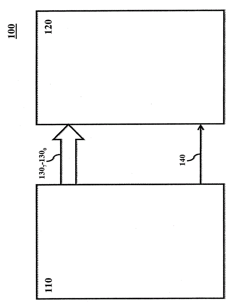
[0022] figure 1 An exemplary computer system 100 is shown having a processing unit and memory devices. Computer system 100 incl...


PUM


Abstract

A method and system for calibrating write timing in a memory device. For example, the method can include receiving a data signal, writing a clock signal and a reference signal. The method can also include detecting a phase shift of the reference signal over time. The phase shift of the reference signal can be used to calibrate the phase difference between the data signal and the write clock signal, wherein the memory device recovers the signal from the data signal based on the calibrated write timing of the data signal and the write clock signal.

Description

technical field [0001] Embodiments of the present invention generally relate to calibration of write timing in memory devices, and more particularly to calibrating write timing of memory devices based on reference signals. Background technique [0002] For example, data communication between a processing unit and a memory device typically involves sending data along signal paths such as wires and traces. In a memory device with a synchronous interface, the processing unit can transmit clock signals and data signals to the memory device. The clock signal is used to determine when the data signal should be latched by the memory device, thereby synchronizing the memory device with the processing unit. For correct data recovery, the memory device must receive the clock signal within a period of time for the clock signal to sample the data signal (i.e., the clock signal must sample the data signal for a period of time corresponding to the data eye of the data signal ). Otherwi...

Claims


Application Information

Patent Timeline
Patent Type & Authority Patents(China)
IPC IPC(8): G06F13/16G06F13/42
CPCG06F13/1689G06F13/4234G11C7/22G11C7/222G11C11/4076
Inventor M·E·李S·M·巴拉卡特W·F·克鲁格徐晓泠T·D·范A·J·奈格伦
Owner ADVANCED MICRO DEVICES INC
Features
  • R&D
  • Intellectual Property
  • Life Sciences
  • Materials
  • Tech Scout
  • Unparalleled Data Quality
  • Higher Quality Content
  • 60% Fewer Hallucinations
Learn More