
Repair device, repair method, and component manufacturing method

A device and component technology, which is applied in the fields of repairing devices and repairing and device manufacturing, can solve problems such as current supply current capacity of difficult devices

Inactive Publication Date: 2012-12-19
SHARP KK
View PDF4 Cites 2 Cited by
  • Summary
  • Abstract
  • Description
  • Claims
  • Application Information

AI Technical Summary

Problems solved by technology

[0018] In this regard, it is also conceivable to connect a power supply in parallel to a plurality of devices that collectively process a plurality of electrical bias processes, but the number of devices that are collectively processed is not about two but about ten or even dozens When there are as many as one, several hundred, etc., it is impossible to ensure sufficient current capacity simultaneously from the power supply under the same stress (voltage) conditions for multiple devices
Even if there is only one device, it is difficult to ensure a sufficient current capacity for the current supply of the device while keeping the power supply capacity as low as possible

Method used


Image

  • Repair device, repair method, and component manufacturing method
  • Repair device, repair method, and component manufacturing method
  • Repair device, repair method, and component manufacturing method

Examples


Embodiment approach 1

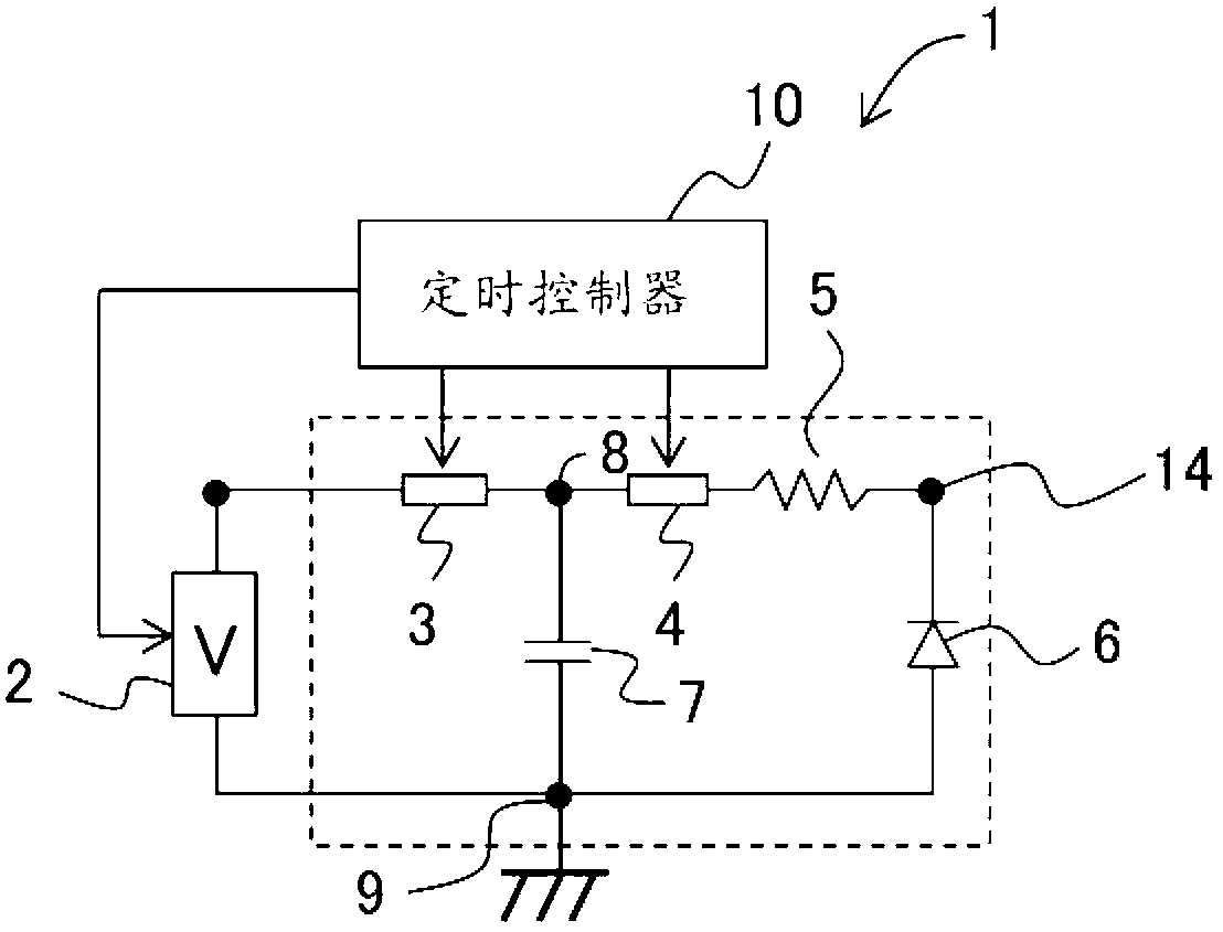
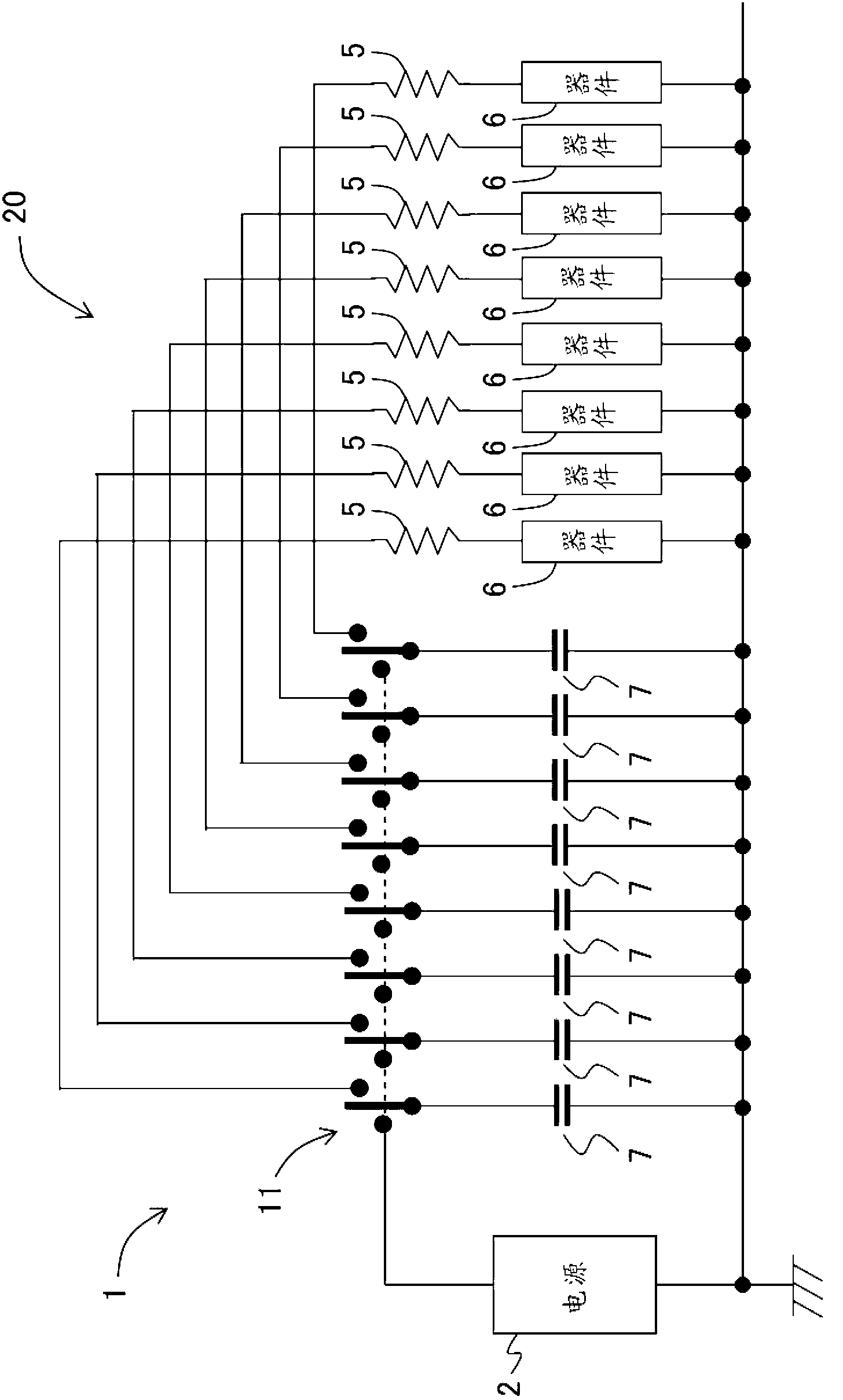
[0127] figure 1 It is a circuit block diagram schematically showing an example of the unit configuration of the repair device in Embodiment 1 of the present invention. In addition, in the repairing device, there is one unit structure example and a portion surrounded by a dotted line, but there are multiple unit structure examples, in particular, three or more, or about ten to several hundred, or even other. above.

[0128] exist figure 1 Among them, in the repairing device 1 according to the first embodiment, one terminal of the high voltage power supply 2 whose output voltage can be freely varied is connected to one end of the application resistor 5 through the high withstand voltage relays 3 and 4 . The other end of the application resistor 5 is connected to one terminal of a device 6 to be inspected and processed. The other terminal of the inspection and processing object device 6 is connected to the other terminal of the high-voltage power supply 2 . The connection p...


PUM


Abstract

The present invention relates to a repair device, a repair method and a component manufacturing method. A plurality of electric biasing treatments is processed all together so as to effectively recover disqualified components to the state of insulation. The repair apparatus (1) which provides an electrical stress for an electric leakage defect part to normalize the state of insulation of the electric leakage defect part is provided with a high voltage power supply (2) served as an electrical stress source, and a voltage applying unit for concurrently applying charge stresses from a plurality of capacitors (7) charged by the high voltage power supply (2) to a plurality of components (6)respectively.

Description

technical field [0001] The present invention relates to, for example, the results of an ESD tolerance test or the results of a normal operation test for inspecting light-emitting elements such as LSI elements, LED elements, and laser elements, and inspecting devices to be processed, and returning defective devices to normal insulation A repairing device and a repairing method in the state, and a method of manufacturing a device using the repairing device. Background technique [0002] Conventionally, a protection diode is connected to the input circuit side of an LSI device, and the ESD resistance of the protection diode is checked. In light-emitting elements such as LED elements and laser elements, the light-emitting element itself has a diode structure. Since this diode structure is composed of a pn structure of a p-type diffusion layer and an n-type diffusion layer, the ESD resistance is different depending on the results of the p-type diffusion layer and the n-type diff...

Claims


Application Information

Patent Timeline
IPC IPC(8): H01L21/67H01L33/00H01L31/18H01L51/56G01R31/00G01R31/12
CPCY02P70/50G01R31/1263H01L21/76868
Inventor 内田练石川真治
Owner SHARP KK
Learn More