Supercharge Your Innovation With Domain-Expert AI Agents!

Radiation-emitting semiconductor body, method for producing a radiation-emitting semiconductor body, and radiation-emitting semiconductor component

A technology that emits radiation and semiconductors. It is applied in the direction of semiconductor devices, electrical solid devices, and printed circuits assembled with electrical components. It can solve problems such as time-consuming and achieve the effect of rapid manufacturing.

Active Publication Date: 2015-11-25
OSRAM OPTO SEMICON GMBH & CO OHG
View PDF6 Cites 0 Cited by
  • Summary
  • Abstract
  • Description
  • Claims
  • Application Information

AI Technical Summary

Problems solved by technology

The manufacturing method is relatively time-consuming due to continuous process control

Method used


Image

  • Radiation-emitting semiconductor body, method for producing a radiation-emitting semiconductor body, and radiation-emitting semiconductor component
  • Radiation-emitting semiconductor body, method for producing a radiation-emitting semiconductor body, and radiation-emitting semiconductor component
  • Radiation-emitting semiconductor body, method for producing a radiation-emitting semiconductor body, and radiation-emitting semiconductor component

Examples


Embodiment Construction

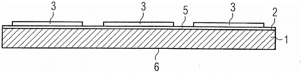
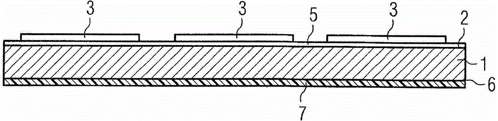
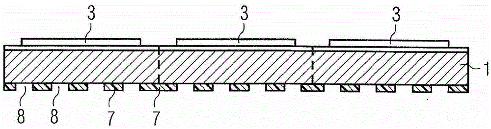
[0053] Elements that are the same, of the same type or have the same effect are provided with the same reference symbols in the figures. The drawings and the dimensional ratios of the elements described in the drawings to each other cannot be regarded as being to scale. Conversely, individual elements, in particular layer thicknesses, can be shown exaggerated for better visibility and / or for better understanding.

[0054] Figure 1A A carrier layer 1 is shown, on whose first main side 2 an epitaxial semiconductor layer sequence 3 is arranged. The carrier layer 1 mechanically stabilizes the semiconductor layer sequence 3 . The epitaxial semiconductor layer sequence 3 has now been structured in chip regions, each chip region then being part of the finished semiconductor body. The epitaxial semiconductor layer sequence 3 has an active region 4 suitable for generating electromagnetic radiation (in Figures 1A to 1G not shown).

[0055] Particularly preferably, the further laye...


PUM


Abstract

A radiation-emitting semiconductor body is provided which, besides an epitaxial semiconductor layer sequence having an active zone that is suitable for generating electromagnetic radiation, has a carrier layer that is intended to mechanically stabilize the epitaxial semiconductor layer sequence. The semiconductor body furthermore has contact structures for electrical contacting of the semiconductor body, which respectively have a volume region and a surface bonding region. The surface bonding region is formed from a material which is different from the material of the volume region.

Description

technical field [0001] The invention relates to a radiation-emitting semiconductor body, a method for producing a radiation-emitting semiconductor body, and a radiation-emitting semiconductor component. Background technique [0002] Reference EP 1 657 757 A2 describes a radiation-emitting semiconductor component with a radiation-emitting semiconductor body which is electrically conductively applied to a chip carrier via electrical contacts on the rear side by means of joining methods, for example ultrasonic friction welding or thermocompression . [0003] To produce the rear contacts, as described, for example, in reference US 2005 / 0247944 A1, the individual electrically conductive contacts are applied successively on the semiconductor body by means of a ball bonder. This production method is relatively time-consuming due to the continuous process control. Contents of the invention [0004] It is an object of the present invention to provide a semiconductor body which is...

Claims


Application Information

Patent Timeline
Patent Type & Authority Patents(China)
IPC IPC(8): H01L33/62H05K3/32H01L33/38H01L33/00
CPCH01L33/40H01L24/73H01L33/0079H01L33/387H01L33/62H01L2224/48091H01L2924/01013H01L2924/01029H01L2924/01042H01L2924/01068H01L2924/01079H01L2924/12036H01L2924/12042H05K2201/10106H05K2201/10969H01L2933/0066H01L2224/92125H01L2224/92227H01L2224/73204H01L2224/16225H01L2224/32225H01L33/0093H01L2924/00014H01L2924/00H01L33/36H01L33/38
Inventor 赫贝特·布伦纳帕特里克·宁斯
Owner OSRAM OPTO SEMICON GMBH & CO OHG
Features
  • R&D
  • Intellectual Property
  • Life Sciences
  • Materials
  • Tech Scout
  • Unparalleled Data Quality
  • Higher Quality Content
  • 60% Fewer Hallucinations
Learn More