Surface plasmon light emitter structure and method of manufacture

a light emitter and surface plasmon technology, applied in the direction of basic electric elements, electrical equipment, semiconductor devices, etc., can solve the problems of relatively poor extraction efficiency of light from semiconductor light sources, delay in the delivery of inexpensive solid-state lighting, etc., to enhance the emission rate, enhance the emission efficiency, and enhance the emission of electromagnetic radiation

Inactive Publication Date: 2005-12-29
CALIFORNIA INST OF TECH
View PDF2 Cites 298 Cited by
  • Summary
  • Abstract
  • Description
  • Claims
  • Application Information

AI Technical Summary

Benefits of technology

[0012] In an alternative specific embodiment, the present invention provides a method for fabricating light emitting devices. The method includes providing a substrate comprising a surface region. The method includes forming a first type semiconductor material overlying the surface region of the substrate and forming a quantum well material (e.g., active region) overlying the semiconductor material. The method forms a second type semiconductor material overlying the quantum well material. A textured interface region is formed between the second type semiconductor material and a metal layer to be formed overlying the second type semiconductor material. Depending upon the embodiment, the textured interface is provided on either the semiconductor material and / or the metal layer. The method includes forming a metal layer including a surface region overlying the second type semiconductor material at a preferred spatial spacing between the surface region and the second type semiconductor material. The preferred spacing is sufficient to cause a coupling between a surface plasmon mode at the surface region of the metal layer and the quantum well material. The textured interface region enhances formation of a first electromagnetic radiation to be derived from the surface plasmon mode. Additionally, the coupling associated with the spatial spacing between the surface region of the metal layer and the second type semiconductor material causes an increase of a level of second electromagnetic radiation to be derived from the quantum well material.
[0016] Moreover, the present invention provides yet another a light emitting semiconductor device. The device has a substrate comprising a surface region and a metal layer overlying the surface region of the substrate. The device has an interface region between the surface region and the metal layer. A textured characteristic is provided at or within a vicinity of the interface region. The device has a spatial spacing between the metal layer and the substrate to cause a coupling between electron-hole pairs generated in the substrate and a surface plasmon mode at the interface region. In a preferred embodiment, the device has a first electrode coupled to the substrate and a second electrode coupled to the metal layer. A voltage source is coupled between the first electrode and the second electrode to generate electromagnetic radiation in the substrate. Preferably, the electromagnetic radiation has been enhanced by the coupling between the electron-hole pairs generated by the substrate and the surface plasmon mode at the interface region.
[0018] Numerous benefits can be achieved using the present invention over conventional techniques. As merely an example, the present invention can provide enhanced emission efficiencies using a surface plasmon coupling effect or like influences that leads to enhancement of electromagnetic radiation emitted from the light emitting device structure. Additionally, the invention can be implemented using conventional materials and process technology. In preferred embodiments, the invention including method and structure can be used with certain conventional light emitting diode structures. In other preferred embodiments, the present method and structures may lead to solid state light sources, which would replace conventional light sources such as fluorescent tubes, light bulbs, etc. Moreover, the present invention including method and device can lead to enhanced emission rates according to certain embodiments. Such enhanced rates may be useful for high speed light emitters for communication applications, optical coupling applications, and others. The present manufacturing technique can also lead to improved throughput, efficiency, and yield. Depending upon the embodiment, one or more of these benefits may be achieved. These and other benefits are described throughout the present specification and more particularly below.

Problems solved by technology

However, the promise of inexpensive solid state lighting has so far been delayed by the relatively poor extraction efficiency of light from semiconductor light sources.

Method used


Image

  • Surface plasmon light emitter structure and method of manufacture
  • Surface plasmon light emitter structure and method of manufacture
  • Surface plasmon light emitter structure and method of manufacture

Examples


Embodiment Construction

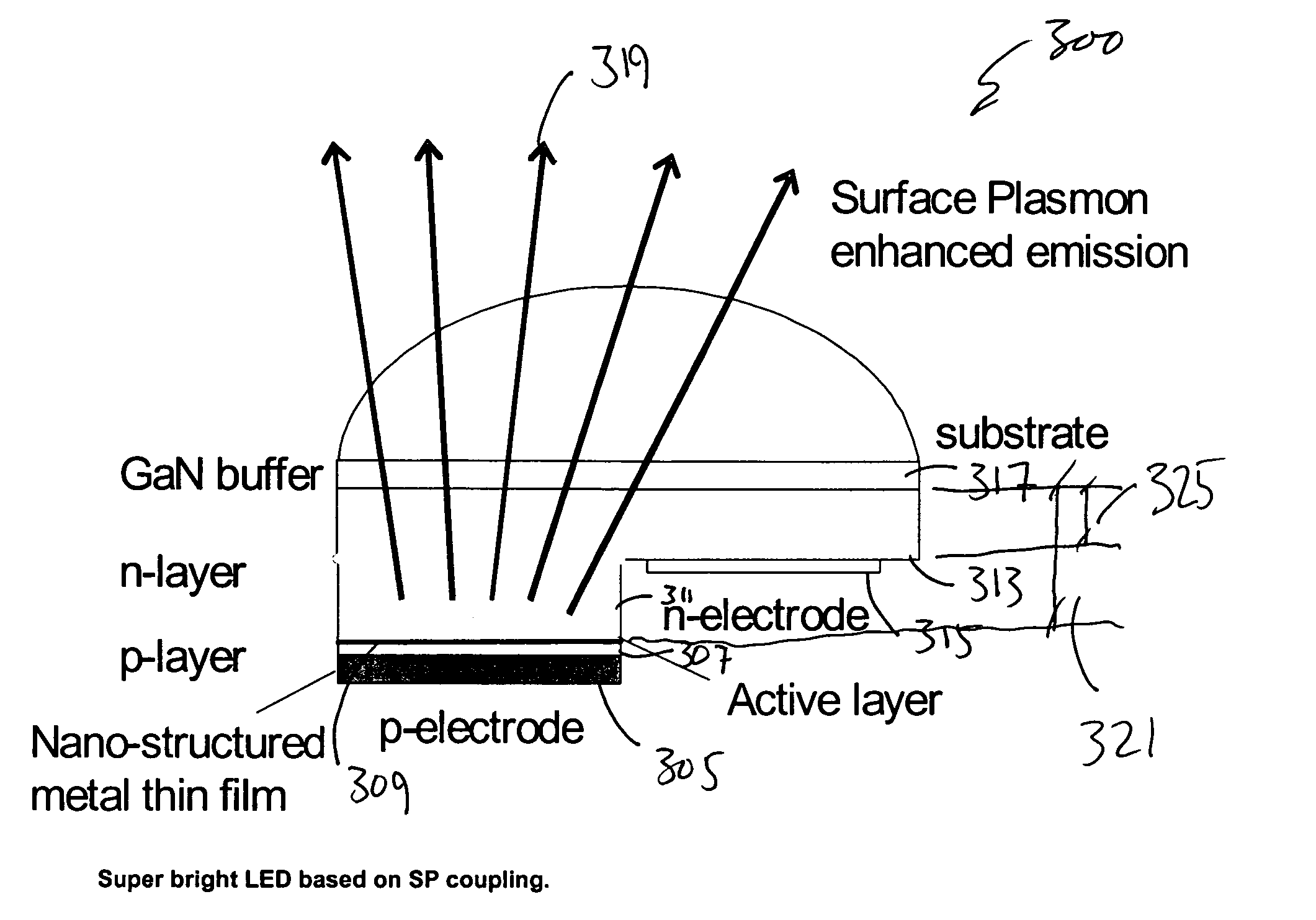
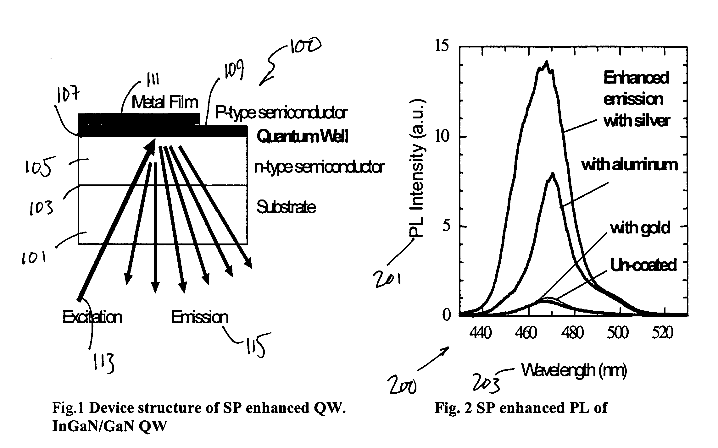
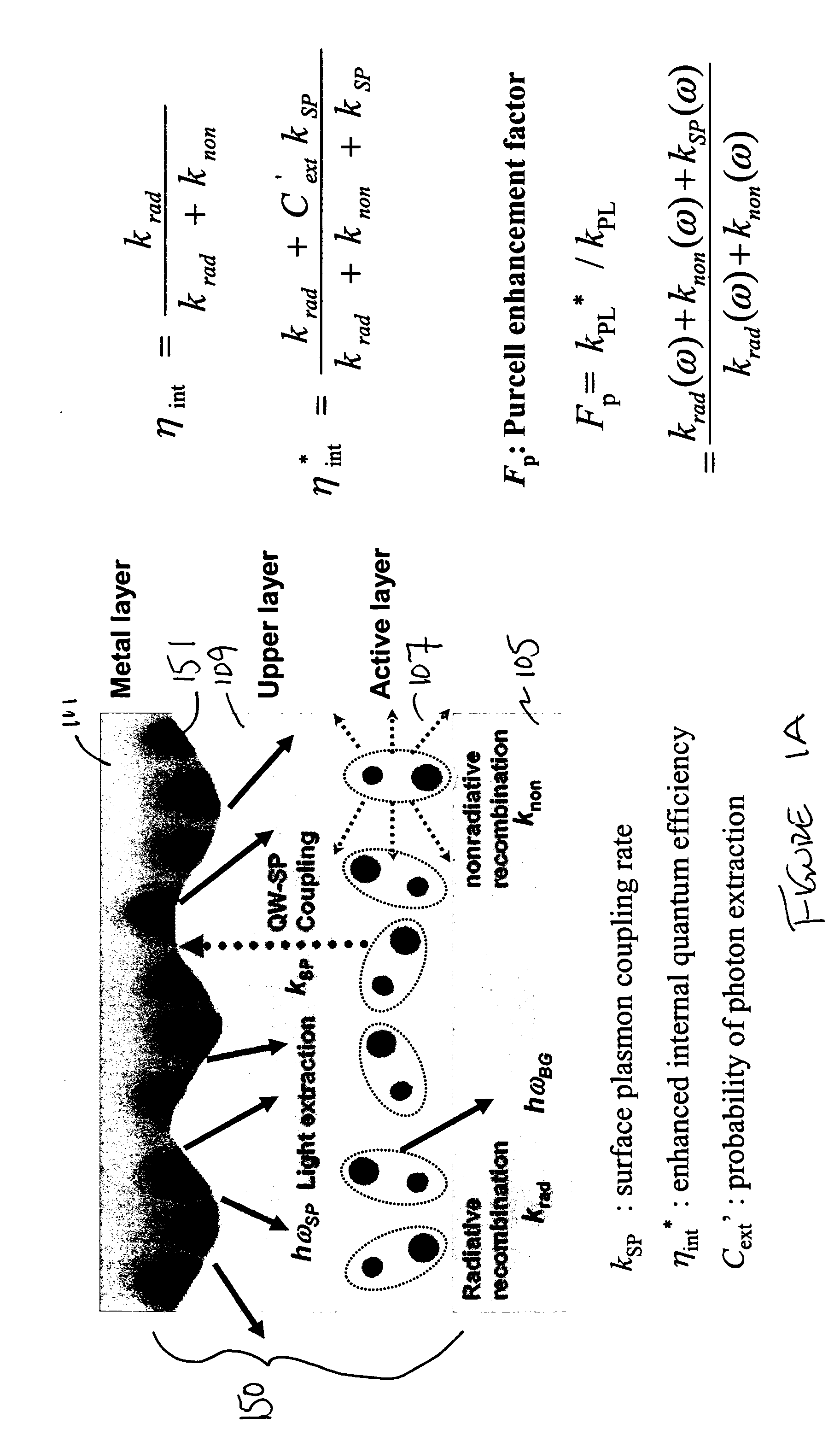
[0031] According to the present invention, techniques for emission of electromagnetic radiation using light emitting diodes and their methods of manufacture are provided. More particularly, the present invention provides a method and structure for a light emitting diode having enhanced characteristics by surface plasmon coupling. Merely by way of example, the invention has been applied to indium gallium nitride (“InGaN”) quantum wells, but it would be recognized that the invention has a much broader range of applicability. For example, the invention can be applied to other semiconductor materials such as silicon (Si), germanium (Ge), silicon carbide (SiC), gallium nitride (GaN), indium gallium nitride (InGaN), aluminum gallium nitride (AlGaN), zinc selenium (ZnSe), zinc cadminum selenium (ZnCdSe), gallium arsenide (GaAs), aluminum gallium arsenide (AlGaAs), indium gallium srdenide (InGaN), gallium phosphide (GaP), indium gallium aluminum phosphide (InGaAlP), alumimun nitride (AlN), ...


PUM

PropertyMeasurementUnit
thicknessaaaaaaaaaa
thicknessaaaaaaaaaa
distanceaaaaaaaaaa

Abstract

A method (and resulting structures) for manufacturing light emitting semiconductor devices. The method includes providing a substrate comprising a surface region and forming a metal layer overlying the surface region of the substrate. In a specific embodiment, the metal layer and the surface region are characterized by a spatial spacing between the metal layer and the substrate to cause a coupling between electron-hole pairs generated in the substrate and a surface plasmon mode at an interface region between the metal layer and the surface region. Additionally, the interface region has a textured characteristic between the surface region and the metal layer. The textured characteristics causes emission of electromagnetic radiation through the surface plasmon mode or like mechanism according to a specific embodiment.

Description

CROSS-REFERENCES TO RELATED APPLICATIONS [0001] The present application claims priority to U.S. Provisional Application Ser. No. 60 / 543,127 (Caltech Docket Number CIT 4041) filed Feb. 10, 2004, commonly assigned, and hereby incorporated by reference herein.STATEMENT AS TO RIGHTS TO INVENTIONS MADE UNDER FEDERALLY SPONSORED RESEARCH OR DEVELOPMENT [0002] Certain rights to the invention herein may be subject to rights under Government Grant AFOSR under Contract Number F49620-03-1-0418.BACKGROUND OF THE INVENTION [0003] The present invention relates generally to emission of electromagnetic radiation using light emitting diodes and their methods of manufacture. More particularly, the present invention provides a method and structure for a light emitting diode having enhanced characteristics by surface plasmon coupling. Merely by way of example, the invention has been applied to indium gallium nitride (“InGaN”) quantum wells, but it would be recognized that the invention has a much broad...

Claims


Application Information

Patent Timeline
Patent Type & Authority Applications(United States)
IPC IPC(8): H01L29/22H01L33/20H01L33/22H01L33/40
CPCH01L33/20H01L33/22H01L33/38H01L2933/0083H01L33/405
Inventor SCHERER, AXELOKAMOTO, KOICHI
Owner CALIFORNIA INST OF TECH
Why Eureka
Try Eureka