Analysis and measurement method for electromagnetic radiation of voltage driven radiation source

A voltage-driven, electromagnetic radiation technology, used in electronic circuit testing, measuring electricity, measuring devices, etc.

Inactive Publication Date: 2013-03-20
JIANGSU SUPERVISION & INSPECTION INST FOR PROD QUALITY
View PDF3 Cites 14 Cited by
  • Summary
  • Abstract
  • Description
  • Claims
  • Application Information

AI Technical Summary

Problems solved by technology

[0007] The purpose of the present invention is to solve the technical problems existing in the existing electromagnetic compatibility measurement, to overcome the defects of the prior art, and to propose a voltage-driven radiation source electromagnetic radiation analysis and measurement method

Method used


Image

  • Analysis and measurement method for electromagnetic radiation of voltage driven radiation source
  • Analysis and measurement method for electromagnetic radiation of voltage driven radiation source
  • Analysis and measurement method for electromagnetic radiation of voltage driven radiation source

Examples


Embodiment Construction

[0042] The present invention will be described in further detail below in conjunction with the accompanying drawings and specific embodiments.

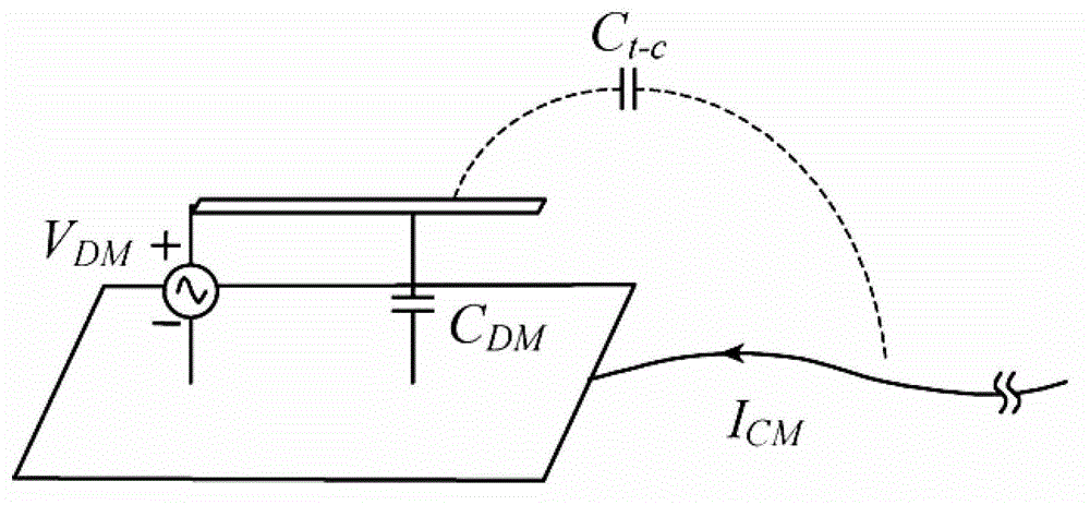
[0043] like figure 1 As shown, V DM is the PCB voltage signal (differential mode signal), C DM Distributed capacitance for the PCB circuit board, C t-c is the distributed capacitance between the radiation cable and the PCB, I CM is the common-mode current of the radiating cable. for figure 1 The radiation model shown can be considered as radiated electromagnetic interference noise caused by the radiation cable itself and the common mode current in the radiation cable. In addition, due to the common mode current in the radiating cable and the PCB voltage signal V DM , PCB distributed capacitance C DM , the distributed capacitance C between the radiation cable and the PCB t-c , Radiating cable input capacitance C in , radiating cable length l, radiating cable common-mode current distribution is related to radiating cable impeda...


PUM


Abstract

The invention discloses an analysis and measurement method for electromagnetic radiation of a voltage driven radiation source. The method is used for analyzing parameters of a PCB (printed circuit board) circuit and a radiation cable test circuit and measuring near field radiation characteristics of the circuits. Considering a small-scale model of a PCB circuit radiation cable, a relation between radiation electromagnetic interference noise and the parameter of the PCB circuit can be established according to a relation between E field intensity of a radiation electromagnetic field and common mode current ICM of the radiation cable; the estimated radiation electromagnetic field is multiplied by 2 to compensate ground reflection under the worst condition in a semiwave darkroom; CM current between the PCB circuit and the radiation cable can be expressed with equivalent CM voltage to obtain the maximum radiation field; a relation between a common mode voltage signal and a PCB voltage signal meets the formula as described in the specification; Ct-c is distributed capacitance between the radiation cable and a PCB; Cin is input capacitance of the radiation cable; and the magnitude of the radiation electromagnetic interference noise can be measured, presstimated and calculated by only measuring circuit parameters in the PCB.

Description

technical field [0001] The present invention relates to a method for analyzing circuit parameters of high-speed PCB circuits and predicting circuit near-field radiation characteristics, especially a method for analyzing and predicting electromagnetic radiation characteristics of high-speed PCB circuits based on voltage-driven circuit parameter current segmentation calibration. It provides a premise for the mechanism judgment and suppression of radiated electromagnetic interference (EMI) noise, and belongs to the field of electromagnetic compatibility technology. Background technique [0002] Modern electrical and electronic products are developing in the direction of miniaturization and intelligence, and the design of the system is becoming more and more complex. Coupled with the parasitic parameters generated by the switching devices in the equipment, the radiation interference of the equipment is becoming more and more serious, and it affects the system's ability to resist ...

Claims


Application Information

Patent Timeline
Patent Type & Authority Applications(China)
IPC IPC(8): G01R31/00G01R31/28G01R29/08
Inventor 陈向阳郭艳萍
Owner JIANGSU SUPERVISION & INSPECTION INST FOR PROD QUALITY
Why Eureka
Try Eureka