Universal single event effect detecting method of memory circuit

A memory circuit and single event effect technology, applied in static memory, instruments, etc., can solve the problems of difficult positioning, multi-bit flipping and statistics, lack of versatility, difficulty in data analysis of memory circuits, etc., to achieve rich test methods and detection functions full effect

Inactive Publication Date: 2013-04-03
BEIJING MXTRONICS CORP +1
View PDF4 Cites 34 Cited by
  • Summary
  • Abstract
  • Description
  • Claims
  • Application Information

AI Technical Summary

Benefits of technology

This patented technology allows us to check if there's any damage done or how well it works over multiple times without having to stop working altogether. It also provides various testing modes such as timing analysis, voltage fluctuation tests, etc., allowing users to study the impact of these factors on their memories. Overall, this technology helps researchers better identify issues early before they become serious problems affecting them.

Problems solved by technology

Technological Problems In this patented technical problem addressed in this patents include difficulty in detecting both single fault effects due to radiation damage from charged particles or defective elements within electronic components such as integrated circuits (IC), which causes malfunctions with reduced functionality and increased costs associated with failure prediction measures like static timing tests. Current methods require extensive effort and cannot provide comprehensive coverage across different types of memories without requiring significant modifications.

Method used


Image

  • Universal single event effect detecting method of memory circuit

Examples


Embodiment Construction

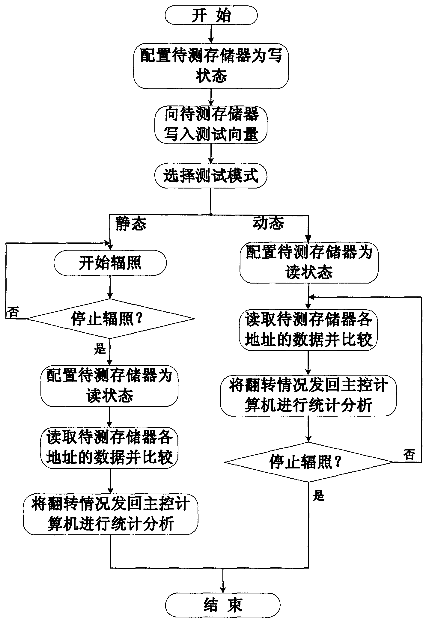
[0025] Such as figure 1 As shown in FIG. 2 , it is a flow chart of the general single event effect detection method for the memory circuit of the present invention. After starting the test, firstly, by configuring the pin signals of the memory device to be tested, the memory to be tested is made to work in three different working modes: write state, read state, or non-read and non-write state.

[0026] In the write state, according to the test instruction, write the test vector ("00", "FF", "55", "AA", "55"+"AA", "00"+" FF”, MARCH, etc.). In the test process, the required test vector can be selected through the input command of the host computer so that the storage state and working state of the unit of the memory circuit are in a specific state, and then the anti-single event effect performance of the memory circuit is comprehensively assessed.

[0027] In the read state, the data output terminal of the memory to be tested is detected, and the received data is compared with...


PUM


Abstract

The invention provides a universal single event effect detecting method of a memory circuit. The universal single event effect detecting method comprises the following steps of (1) configuring a memory to be detected to be in a write state, and writing into a test vector; and then arranging the memory to be detected in a radiation environment; (2) if a dynamic test is conducted, configuring the memory to be detected to be in a read state, reading out data stored in each address unit and comparing the read-out data with the written-in data, using the quantity of address units with different comparing results as a total error count, and further analyzing a condition that each address unit generates 2-bit or more than 2-bit data flipping; and (3) if a static test is conducted, configuring the memory to be detected to be in a non-read non-write state; after irradiation particles accumulated in an irradiation process reach a standard, sequentially reading out data in each address unit and comparing with the written-in data; and using the quantity of the address units with the different comparing results as the total error count. In the irradiation process, working current of the memory to be detected can be monitored in real time. Latch is implemented when the working current exceeds 1.5 times of normal working current.

Description


Claims


Application Information

Patent Timeline
Owner BEIJING MXTRONICS CORP
Why Eureka
Try Eureka