Capacitive touch screen, manufacturing method thereof, and touch display device
A capacitive touch screen and electrode technology, which is applied in the direction of electrical digital data processing, optics, instruments, etc., can solve the problems of affecting the visual effect of the surface and large dielectric constant, so as to improve the visual effect of the surface, improve the reliability of the product, and reduce the process steps Effect
- Summary
- Abstract
- Description
- Claims
- Application Information
AI Technical Summary
Problems solved by technology
Method used
Image
Examples
Embodiment 1
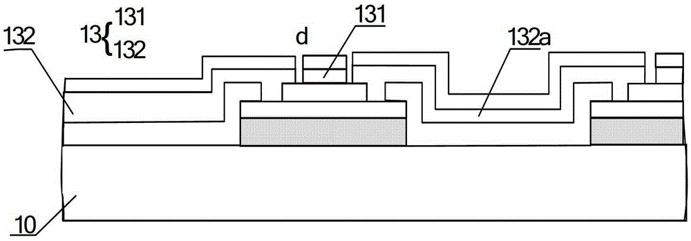
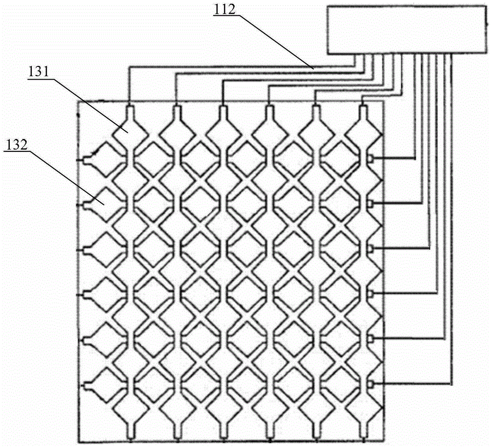
[0044] An embodiment of the present invention provides a capacitive touch screen, such as figure 2 and image 3As shown, it includes: a transparent substrate 10 and a patterned transparent conductive layer 13, and the transparent conductive layer 13 is disposed on the transparent substrate 10, including: a first conductive layer extending along a first direction (the longitudinal direction as shown in the figure). The sensing line 131 and the second sensing line 132 extending along a second direction (such as a transverse direction perpendicular to the longitudinal direction),
[0045] Wherein, the first sensing line 131 remains continuous in the first direction, and is a series of sequentially connected electrodes; the second sensing line 132 includes a plurality of independent electrodes 132a separated from each other, and the independent electrodes 132a cross the first electrode in a bridging manner. The sensing lines 131 are connected to each other;
[0046] The gap d b...
Embodiment 2
[0063] The present invention also provides a manufacturing method of a capacitive touch screen, referring to Figure 2-5 , the touch screen includes: a transparent substrate 10, a transparent surface protection layer 14, a transparent conductive layer 13, an insulating layer 12, a second transparent conductive layer 15, and a metal layer 11 are sequentially arranged on the transparent substrate 10 from top to bottom, such as Figure 6 As shown, the method includes:
[0064] Step 101, such as Figure 7 As shown, the metal layer 11 and the second transparent conductive layer 15 are fabricated on the transparent substrate 10, and several groups of bridges are formed in the visible area of the capacitive touch screen by using a patterning process. Each group of bridges includes a plurality of metal layers arranged at intervals along the second direction. The bridge 111 forms a metal trace 112 in the bonding area 20 of the capacitive touch screen, and at the same time forms a tr...
PUM
| Property | Measurement | Unit |
|---|---|---|
| relative permittivity | aaaaa | aaaaa |
| relative permittivity | aaaaa | aaaaa |
Abstract
Description
Claims
Application Information


