
An electrostatic discharge protection circuit

A technology of electrostatic discharge protection and circuit, which is applied in the direction of circuits, electrical components, electric solid devices, etc., can solve the problem that the electrostatic discharge protection cannot be turned on at the same time, and achieve the effect of improving the level of electrostatic discharge protection

Active Publication Date: 2016-04-06
SEMICON MFG INT (SHANGHAI) CORP
View PDF5 Cites 0 Cited by
  • Summary
  • Abstract
  • Description
  • Claims
  • Application Information

AI Technical Summary

Problems solved by technology

It is precisely because the resistance formed by the part of the NMOS region close to the pick-up region is smaller than the resistance formed between the central part of the NMOS region and the pick-up region, the different fingers cannot simultaneously turn on the electrostatic discharge protection

Method used


Image

  • An electrostatic discharge protection circuit
  • An electrostatic discharge protection circuit
  • An electrostatic discharge protection circuit

Examples


Embodiment Construction

[0018] In the following description, numerous specific details are given in order to provide a more thorough understanding of the present invention. It will be apparent, however, to one skilled in the art that the present invention may be practiced without one or more of these details. In other examples, some technical features known in the art are not described in order to avoid confusion with the present invention.

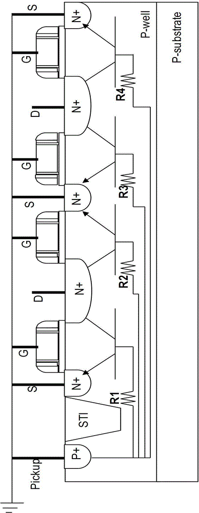
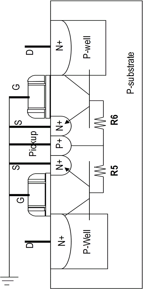
[0019] In order to thoroughly understand the present invention, detailed steps will be provided in the following description, so as to illustrate the electrostatic discharge protection circuit proposed by the present invention that can be turned on uniformly. Obviously, the practice of the invention is not limited to specific details familiar to those skilled in the semiconductor arts. Preferred embodiments of the present invention are described in detail below, however, the present invention may have other embodiments besides these detailed descriptions.

[0...


PUM


Abstract

The invention provides a static discharge protection circuit which is characterized by comprising a plurality of N-metal-oxide-semiconductor (NMOS) transistors. The adjacent NMOS transistors share source diffusion zones or drain diffusion zones. P traps are formed below the drain diffusion zones. A picking area is formed in the central area of the shared source diffusion zones. Grids and sources of the NMOS transistors are grounded. The picking area is also grounded. According to the static discharge protection circuit, when static discharge occurs, each finger in a grounded-gate N-metal-oxide-semiconductor (GGNMOS) simultaneously starts static discharge protection, and improves static discharge protection level measured by human body model (HBM).

Description

technical field [0001] The invention relates to an electrostatic discharge protection circuit, in particular to an electrostatic discharge protection circuit that can be turned on uniformly. Background technique [0002] When an integrated circuit (IC) starts to operate, high energy from the outside is applied to the IC, and a momentary electrostatic discharge (ESD) phenomenon occurs in the IC. The ESD generates a momentary high voltage inside the IC, which causes breakdown of the gate oxide, causing the IC to fail. [0003] The commonly used ESD protection circuit in the prior art is a gate-grounded NMOS (GateGroundedNMOS), such as figure 1 As shown, in the NMOS region of GGNMOS, the source S and the gate G are grounded, and the pickup region (Pickup) is also grounded, and the NPN junction formed between each pair of source S and drain D is connected to the pickup region. The formed resistors are R1, R2, R3 and R4 respectively, and the NPN junction formed between each pai...

Claims


Application Information

Patent Timeline
Patent Type & Authority Patents(China)
IPC IPC(8): H01L27/02H01L21/82
Inventor 甘正浩张莉菲
Owner SEMICON MFG INT (SHANGHAI) CORP
Learn More