Wafer-level light emitting diode package and method of fabricating the same
A technology of light-emitting diodes and packages, which is applied in the field of wafer-level light-emitting diode packages and its manufacturing, and can solve problems such as limiting the extraction efficiency of light-emitting unit structures
Active Publication Date: 2013-05-22
SEOUL SEMICONDUCTOR
View PDF5 Cites 90 Cited by
- Summary
- Abstract
- Description
- Claims
- Application Information
AI Technical Summary
Problems solved by technology
[0009] Since an AC-LED includes a light emitting unit on a growth substrate (for example, on a sapphire substrate),
Method used
View moreImage
Smart ImageViewing Examples

Examples
 PUM
 Abstract
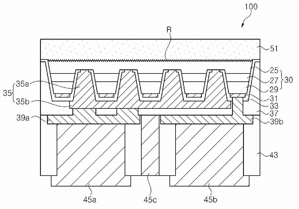
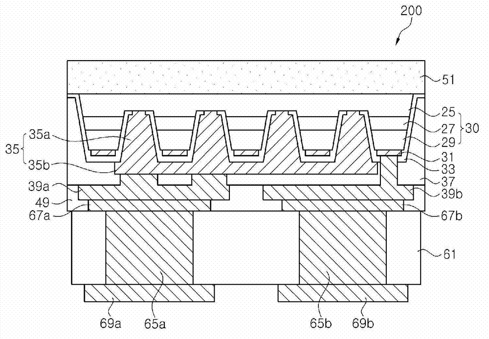
Exemplary embodiments of the present invention provide a wafer-level light emitting diode (LED) package and a method of fabricating the same. The LED package includes a semiconductor stack including a first conductive type semiconductor layer, an active layer, and a second conductive type semiconductor layer; a plurality of contact holes arranged in the second conductive type semiconductor layer and the active layer, the contact holes exposing the first conductive type semiconductor layer; a first bump arranged on a first side of the semiconductor stack, the first bump being electrically connected to the first conductive type semiconductor layer via the plurality of contact holes; a second bump arranged on the first side of the semiconductor stack, the second bump being electrically connected to the second conductive type semiconductor layer; ; and a protective insulation layer covering a sidewall of the semiconductor stack.
Description
technical field [0001] The present invention relates to a light-emitting diode package and its manufacturing method, more specifically, to a wafer-level light-emitting diode package and its manufacturing method. Background technique [0002] A light emitting diode (LED) is a semiconductor device including an N-type semiconductor and a P-type semiconductor and emitting light through recombination of holes and electrons. Such LEDs have been used in a wide range of applications such as display devices, traffic lights, and backlight units. In addition, considering potential advantages of lower power consumption and longer life than current electric bulbs or fluorescent lamps, the application range of LEDs has been expanded to general lighting by replacing current incandescent lamps and fluorescent lamps. [0003] LEDs can be used in LED modules. The LED module is manufactured through a process of manufacturing LED chips at a wafer level, a packaging process, and a modulation p...
Claims
Login to View More Application Information
Patent Timeline
 IPC IPC(8): H01L33/44H01L33/02H01L33/62
CPCH01L33/46H01L25/0753H01L33/20H01L33/0079H01L33/387H01L33/505H01L33/62H01L33/382H01L27/153H01L2933/0033H01L25/0756H01L27/156H01L33/005H01L33/0093H01L33/38H01L33/486H01L2924/0002H01L2924/00
Inventor 徐源哲葛大成
Owner SEOUL SEMICONDUCTOR
Features
- Generate Ideas
- Intellectual Property
- Life Sciences
- Materials
- Tech Scout
- Unparalleled Data Quality
- Higher Quality Content
- 60% Fewer Hallucinations
Learn More Browse by: Latest US Patents, China's latest patents, Technical Efficacy Thesaurus, Application Domain, Technology Topic, Popular Technical Reports.
© 2025 PatSnap. All rights reserved.Legal|Privacy policy|Modern Slavery Act Transparency Statement|Sitemap|About US| Contact US: help@patsnap.com