An Integrated Directional Coupler Based on Standard CMOS Technology

A directional coupler and process technology, applied in the direction of waveguide-type devices, circuits, connecting devices, etc., can solve the requirements of miniaturization and portability of mobile communication systems that cannot meet the requirements of system integration, and cannot realize directional couplers. and other problems, to achieve the effect of low cost, small metal wire spacing, and compact overall structure

Inactive Publication Date: 2015-07-29
PEKING UNIV
View PDF4 Cites 0 Cited by
  • Summary
  • Abstract
  • Description
  • Claims
  • Application Information

AI Technical Summary

Problems solved by technology

In order to be able to integrate directional couplers on-chip, some people have used some special processing techniques before, such as Shim, S., etc. (Shim, S., Hong, S., "A CMOS Power Amplifier With Integrated-Passive-Device Spiral-Shaped Directional Coupler for Mobile UHF RFID Reader, "Microwave Theory and Techniques, IEEE Transactions on, vol.PP, no.99, pp.1, 0) sets forth a kind of directional coupler utilizing IPD (integrated passive device) technology to make, Although the volume is small, the special process technology used is not compatible with the standard CMOS process, the cost is high, the processing process is complicated, and the on-chip integrated directional coupler cannot be realized, and the practicability is poor
[0004] At present, the existing technology has not well solved the problem of preparing directional couplers under the standard CMOS process, which greatly limits the application of these technologies, such as the inability to meet the requirements of miniaturization and portability in the field of mobile communication systems etc.; while some achieve the goal of miniaturization, they are manufactured using special processes, which are costly and cannot meet the requirements of system integration

Method used


Image

  • An Integrated Directional Coupler Based on Standard CMOS Technology
  • An Integrated Directional Coupler Based on Standard CMOS Technology
  • An Integrated Directional Coupler Based on Standard CMOS Technology

Examples


Embodiment Construction

[0034] The present invention will be further described below through the embodiments and in conjunction with the accompanying drawings.

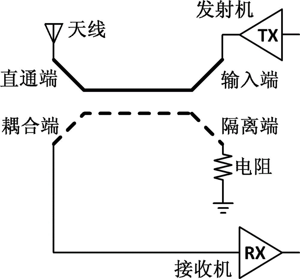
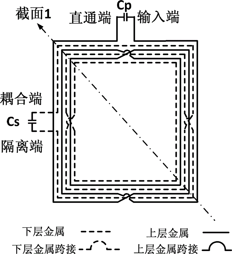
[0035] The integrated directional coupler of this embodiment can be realized on a standard CMOS process or a standard BiCMOS process, and the specific structure of the integrated directional coupler is as follows image 3 , Figure 4 and Figure 5 shown, where image 3 is the top view of the directional coupler layout, Figure 4 for image 3 Sectional view of the middle section 1, Figure 5 Schematic diagram of the crossover of adjacent coils.

[0036] Such as image 3 As shown, the directional coupler includes an upper layer coil (indicated by a solid line) and a lower layer coil (indicated by a dashed line). Both layers of coils are square in shape and have a concentric multi-turn structure, and the two ends of the coil are drawn out from the outermost circle (or the innermost circle). The two ends of the upper coil are respectivel...


PUM


Abstract

The present invention provides a full-on-wafer integrated directional coupler technology for a standard CMOS process and an integrated circuit, belonging to the field of radio frequency communication technologies. The core of the present invention is: a standard CMOS process technology is used, and a CMOS integrated directional coupler is formed of a coil 1 formed by winding a metal wire of an upper layer, a coil 2 formed by winding a metal wire of a lower layer, two tuning capacitor arrays and a matching resistor; two ports of the coil 1 are a direct end and an input end, and two ports of the coil 2 are a coupled end and an isolated end; an angle of 90° exists between the ports of the coil 1 and the ports of the coil 2; the coil 1 is formed by winding metal of a high layer, the coil 2 is formed by winding metal of a bottom layer, the insertion loss is small, and the isolation is large; a capacitor between the direct end and the input end is used for frequency tuning; a capacitor between the coupled end and the isolated end is used for isolation tuning; the coil 1 and the coil 2 adopt a three-dimensional structure, the metal wire of the upper layer and the metal wire of the lower layer partially overlap, and the change of the coil shape, the number of turns, and the line width, the use of different metal layers and the extent of the overlapping between metal wires of different layers may flexibly change performance parameters such as insertion loss, isolation, and coupling. The standard CMOS process integrated directional coupler implemented by the present invention is characterized in that single chip integration on the silicon-based CMOS / BiCMOS process is enabled, the insertion loss is small, the isolation is large, the directivity is good, the tuning performance is strong, the applicability is strong, and the cost is low.

Description

Technical field [0001] The invention belongs to the technical field of radio frequency integrated circuits, and relates to a directional coupler, in particular to an all-on-chip integrated directional coupler based on a standard CMOS process. Background technique [0002] Directional Coupler (Directional Coupler) is a widely used radio frequency device, which can be used for signal isolation, signal separation, etc., so that the radio frequency receiver and transmitter can work in the same frequency band at the same time. The principle of directional coupler applied to transceiver system is as follows: figure 1 As shown, "Input" (Input) is connected to the transmitter output (TX), "Direct" (Direct) is connected to the antenna (Antenna), "Coupled" (Coupled) is connected to the receiver input (RX), "Isolation Terminal" (Isolated) is connected to the matching resistor (Res). Among them, the loss between the input end and the through end is "Insertion Loss", the loss between t...

Claims


Application Information

Patent Timeline
Patent Type & Authority Patents(China)
IPC IPC(8): H01P5/18
CPCH01P5/187
Inventor 叶乐汪佳逸廖怀林黄如
Owner PEKING UNIV
Why Eureka
Try Eureka