

Copper foil and manufacturing method therefor, copper foil with carrier and manufacturing method therefor, printed circuit board, and multilayer printed circuit board
A technology for printed circuit boards and carrier foils, which is applied in the manufacture of printed circuit precursors, printed circuits, and printed circuit manufacturing. It can solve the problems that the surface roughness of copper foil is not necessarily smooth and cannot meet the requirements of copper foil, and achieve excellent high-frequency characteristics. Effect
Inactive Publication Date: 2013-06-12
FURUKAWA ELECTRIC CO LTD
View PDF10 Cites 14 Cited by
- Summary
- Abstract
- Description
- Claims
- Application Information
AI Technical Summary
Problems solved by technology
[0009] In this way, only the surface roughness Rz of the carrier foil is specified, and the surface roughness of the copper foil deposited on it is not necessarily smooth, and sometimes it cannot meet the requirements of copper foil for printed circuit boards forming fine patterns.
Method used
View moreImage
Smart ImageViewing Examples

Examples
Embodiment 1~8)
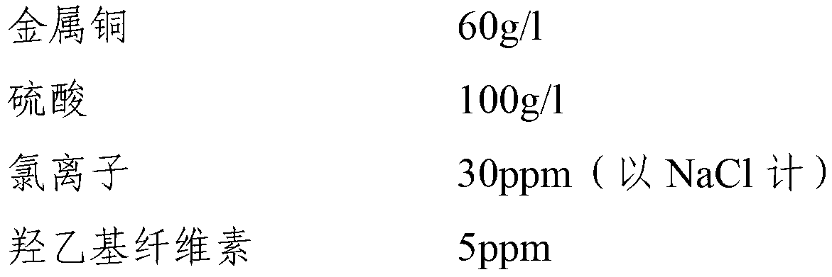
[0069] Plating solution
[0070] ·Bath composition:
[0071]
[0072] ·Bath temperature 58℃
[0073] ·Current density 5~50A / dm 2
[0074] Through the plating solution composed of the above plating bath, the current density and time were changed, and carrier copper foils (35 μm) with different average spacing Sm values were produced on the ground titanium drum (Examples 1-8).
[0075] Table 1 shows the average pitch Sm of the rough surface (portion in contact with the plating solution) of the electrolytic copper foils of Examples 1 to 8 measured.
Login to View More PUM
| Property | Measurement | Unit |
|---|---|---|
| surface roughness | aaaaa | aaaaa |
| thickness | aaaaa | aaaaa |
| surface roughness | aaaaa | aaaaa |
Abstract
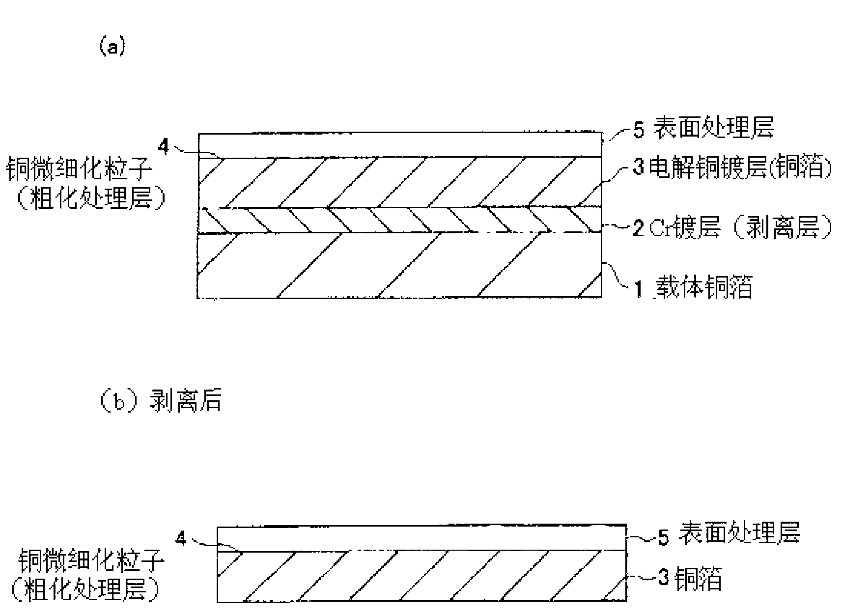
Provided is a copper foil with carrier capable of providing wirings of line / space=15 [mu] m / 15 [mu] m or less on a printed circuit board on which copper foils are laminated. Also provided are a printed circuit board and a multilayer printed circuit board capable of providing wirings with fine patterns of line / space=15 [mu] m / 15 [mu] m or less using the copper foil. A copper foil with carrier obtained by laminating a release layer and a copper foil in this order on a carrier foil having an average interval Sm of 25 [mu] m or more between irregularities of a substrate crest on the surface, the Sm being defined in JIS-B-06012-1994, and by laminating a release layer and a copper foil in this order on a carrier foil which is a copper foil obtained by peeling the former copper foil from the former carrier foil, wherein the interval between irregularities of a substrate crest on the surface of the carrier foil on which copper foils are laminated is 25 [mu]m or more as the average interval Sm defined in JIS-B-06012-1994. A roughening process layer and a surface treatment layer are laminated in this order on the surface of the copper foil as needed.
Description
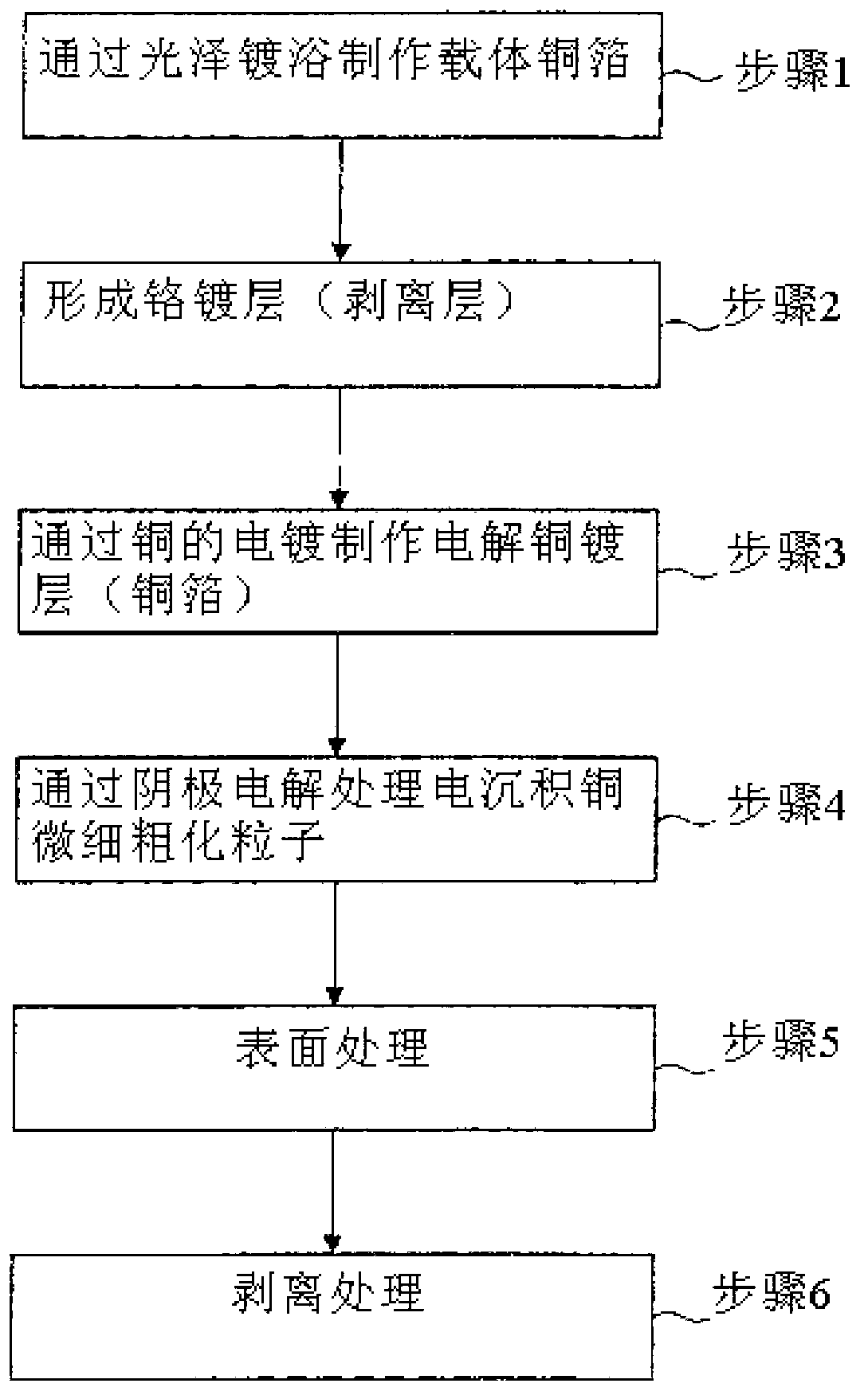
technical field [0001] The present invention relates to a copper foil or a copper foil with a carrier, in particular to a copper foil or a copper foil with a carrier suitable for use in the preparation of a high-density micro-wiring printed circuit board or a multilayer printed circuit board and a preparation method thereof. [0002] Moreover, this invention relates to the printed wiring board which used the said copper foil or the said copper foil with a carrier, and a multilayer printed wiring board. Background technique [0003] As the copper foil used for high-density fine wiring (fine pattern) applications, a copper foil having a thickness of 1 to 9 μm, particularly preferably 1 to 5 μm, is used. [0004] Such thin copper foils used in fine graphic applications are mainly on the market as copper foils with carriers. The copper foil with a carrier is produced by using an electrolytic copper foil as a carrier foil, providing a peeling layer of 1 μm or less on the carrier...
Claims
Login to View More Application Information
Patent Timeline
 Patent Type & AuthorityApplications(China)
IPC IPC(8): C25D1/04C25D7/06H05K1/09
CPCC25D1/04C25D5/12C25D5/48H05K3/025Y10T428/12493Y10T428/12431C25D5/627C25D5/605C25D5/611B32B15/043H05K3/007
Inventor川上昭
OwnerFURUKAWA ELECTRIC CO LTD