Partial inter-locking metal contact structure for semiconductor devices and method of manufacture

a metal contact and semiconductor technology, applied in semiconductor devices, semiconductor/solid-state device details, electrical apparatus, etc., can solve the problems of poor mechanical integrity of deep submicron metal studs, unsatisfactory electro-migration resistance of beol interconnects, and problems that become more severe, so as to enhance the structural integrity of studs and enhance the mechanical strength of metal interconnects , improve the electro-migration resistance of beol

Inactive Publication Date: 2005-05-26
IBM CORP
View PDF10 Cites 22 Cited by
  • Summary
  • Abstract
  • Description
  • Claims
  • Application Information

AI Technical Summary

Benefits of technology

[0013] In the satisfaction of the above objects, a “Lego”-like inter-locking contact structure and method for fabricating the same is provided for high wiring density semiconductors characterized in that the contact liner formed in the via extends only partially into the adjacent wire level. As a consequence, current crowding and related reliability problems associated with conventional prior art interconnect structures is avoided and structural integrity of the stud structure is enhanced.
[0014] A “Lego”-like stud structure with a “crown” of liner extending partially into a next wire level significantly enhances the mechanical strength of metal interconnect. Besides, it also improves the electro-migration resistance of BEOL due to a relatively high liner resistance which forces electrons to go around the fence and then flow down through the stud. In this case, current crowding effect is prevented resulting in less electromigration.
[0015] According to an aspect of the invention, there is provided a semiconductor interconnect structure and method of manufacture, the structure comprising first level of metal conductor and second level of metal conductor and one level of insulator material formed therebetween, the structure further comprising a dielectric metal contact via formed at the insulator material level for electrically connecting the first metal and second metal conductors, wherein the metal contact via includes metal liner material surrounding the metal contact via, a portion of said metal liner extending partially into an adjacent metal level of the first and second metal levels, in interlocking relation therewith to enhance mechanical strength of the semiconductor interconnect structure and improve electromigration resistance.
[0016] According to another aspect of the invention, there is provided a semiconductor capacitor device and method of manufacture, the device comprising a first layer of conductor material forming a bottom node and a first insulator material layer formed thereon; a plurality of metal contact studs formed on said first layer of conductor material having lined sidewall portions extending upwards above a top surface of said insulator material; a second insulator layer formed on said first insulator material layer and conforming to said upward extending lined sidewall portions and, a second layer of conductor material forming a top node on top said second insulator layer, wherein an area density of said capacitor device is improved.
[0017] According to a further aspect of the invention, there is provided a semiconductor heat sink structure and method of manufacture, the heat sink structure comprising: a first layer of heat sink material; a layer of insulator material formed on the first heat sink material layer; a plurality of contact studs extending upwards from the heat sink material layer through the insulator material layer, the contact studs having sidewall portions and filled with heat sink material to improve area density of the heat sink structure.
[0018] Advantageously, the novel “crown” shape of the Lego-like liner structure that is fabricated to extend in an upward direction may be employed for other integrated circuit applications including forming capacitor (e.g., MIMCAP) and heat sink structures due to its increased surface area.

Problems solved by technology

Two major problems encountered in this area today are poor mechanical integrity of deep submicron metal studs, and unsatisfied electro-migration resistance in BEOL interconnects.
The problem becomes more severe when porous low-k material is used.
This not only creates reliability concerns, but also slows down the signal propagation speed of the structure.
Moreover, each of the metal and stud formations taught in the prior art as shown in FIG. 1 and FIG. 2 fail to improve stud mechanical strength, nor to enhance electromigration effect.
This failure may be revealed as broken barrier materials, which will eventually degrade the reliability of the circuits.

Method used


Image

  • Partial inter-locking metal contact structure for semiconductor devices and method of manufacture
  • Partial inter-locking metal contact structure for semiconductor devices and method of manufacture
  • Partial inter-locking metal contact structure for semiconductor devices and method of manufacture

Examples


Embodiment Construction

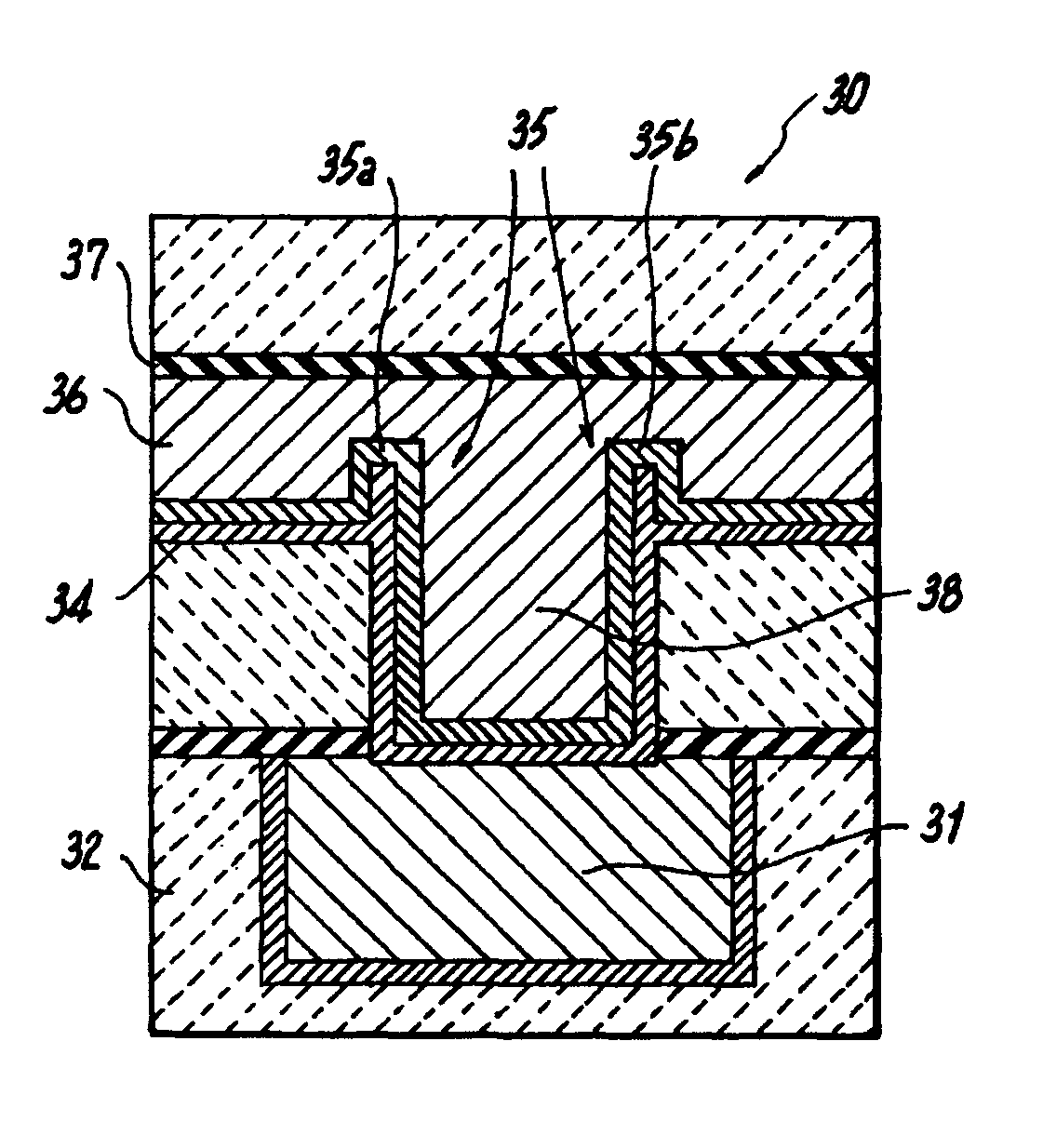
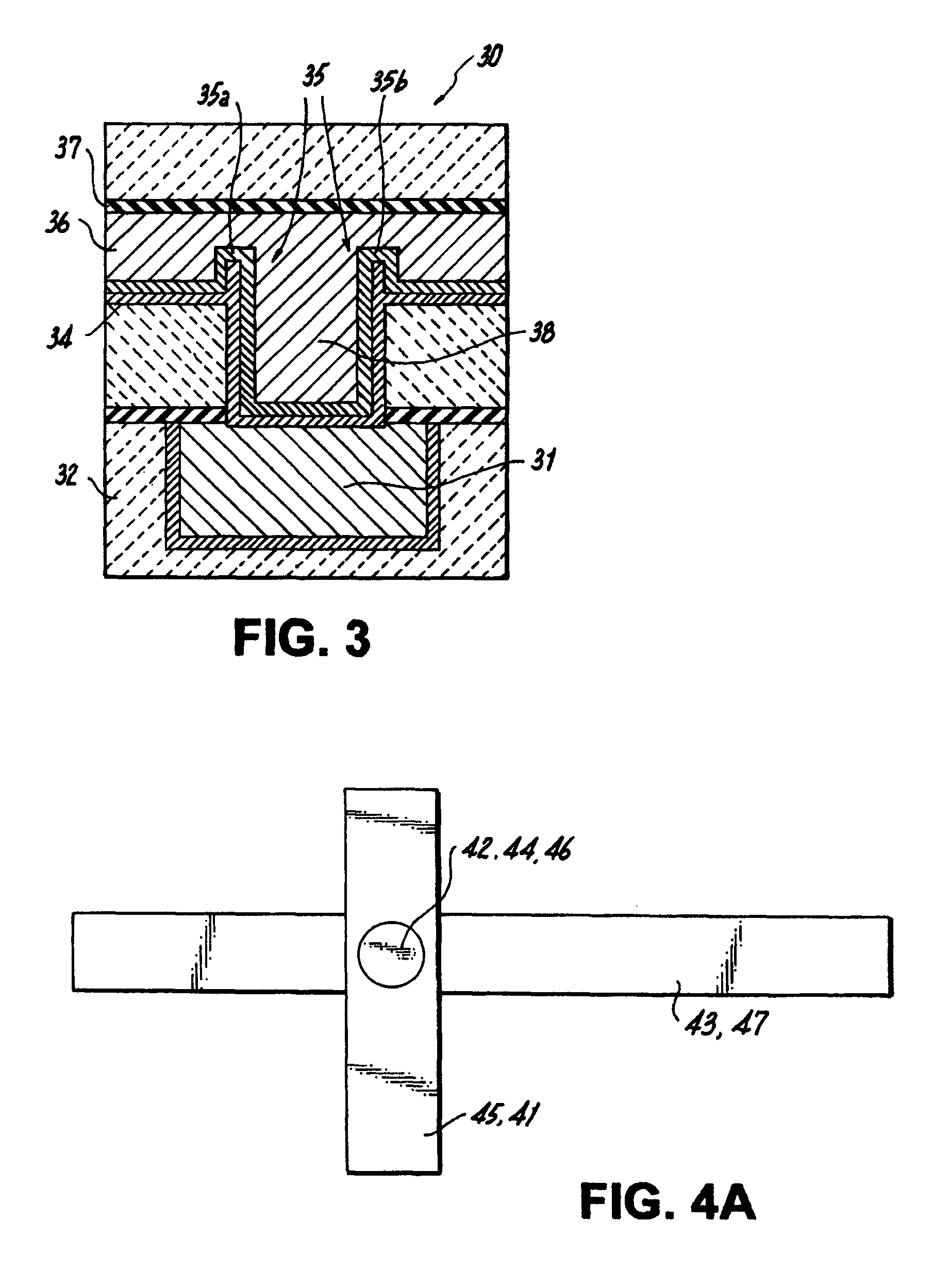
[0030] According to the invention, a method of forming new studs having “Lego”-like inter-locking contact structure is proposed. A schematic representation of a cross-sectional interconnect structure 30 according to the current invention is shown in FIG. 3.

[0031] As illustrated in FIG. 3, the interconnect structure 30 includes a top metal line, 36 connected to a bottom metal line, 31, through a metal via, 38, and these metallic interconnects are embedded in a low-k dialectic material, 32. Additionally, these metal interconnects are enclosed with diffusion barriers, including a contact liner 34 and 35, and a cap insulator, 37, in order to prevent out-diffusion of the metallic atoms into the dielectric material, 32. However, as shown in FIG. 3, the diffusion barrier portions 35a and 35b formed in the via extends only partially into the adjacent wire level 36.

[0032] A comparison of the structure and a conventional one is illustrated in FIGS. 4(A)-4(C). In FIG. 4(A) a top view is pres...


PUM


Abstract

A structure and method of fabricating a “Lego”-like interlocking contact for high wiring density semiconductors is characterized in that the barrier liner formed in the contact via extends only partially upwards into the adjacent wire level. As a consequence, current crowding and related reliability problems associated with conventional prior art interconnect structures is avoided and structural integrity of the contact via (metal stud) structure is enhanced. The novel “crown” shape of the Lego-like interlocking contact structure that is fabricated to extend in an upward direction may be employed for other integrated circuit applications including forming capacitor (e.g., MIMCAP) and heat sink structures due to its increased surface area.

Description

BACKGROUND OF THE INVENTION [0001] 1. Field of the Invention [0002] The present invention relates to semiconductor and integrated circuit structures generally and, particularly to a novel metal contact structure and method that exhibits enhanced mechanical integrity and electromigration resistance in BEOL interconnects comprising the structures. [0003] 2. Description of the Prior Art [0004] As millions and millions of devices and circuits are squeezed on a semiconductor chip, the wiring density and the number of metal levels are both increased generation after generation. In order to provide low RC for high signal speed, low-k dielectric and copper lines become necessary. The quality of thin metal wirings and studs formed by a Damascene process is extremely important to ensure yield and reliability. Two major problems encountered in this area today are poor mechanical integrity of deep submicron metal studs, and unsatisfied electro-migration resistance in BEOL interconnects. The pro...

Claims


Application Information

Patent Timeline
Patent Type & Authority Applications(United States)
IPC IPC(8): H01L21/768H01L23/367H01L23/522H01L23/528
CPCH01L21/76805H01L21/76844H01L21/76847H01L21/76877H01L23/3677H01L23/5223H01L2924/0002H01L23/5226H01L23/5283H01L2924/00
Inventor YANG, CHIH-CHAOCLEVENGER, LAWRENCE A.DALTON, TIMOTHY J.HSU, LOUIS LU-CHENRADENS, CARLWONG, KEITH KWONG-HON
Owner IBM CORP
Why Eureka
Try Eureka