A kind of manufacturing process of step formwork

A technology of making crafts and steps, which is applied in the field of making crafts of step templates to achieve the effect of high position accuracy

Inactive Publication Date: 2016-12-14
KUN SHAN POWER STENCIL
View PDF6 Cites 0 Cited by
  • Summary
  • Abstract
  • Description
  • Claims
  • Application Information

AI Technical Summary

Problems solved by technology

For the local thickening technology, the focus is on the alignment accuracy during the exposure down step after electroforming

Method used


Image

  • A kind of manufacturing process of step formwork
  • A kind of manufacturing process of step formwork
  • A kind of manufacturing process of step formwork

Examples


Embodiment Construction

[0057] Embodiments of the present invention are described in detail below, examples of which are shown in the drawings, wherein the same or similar reference numerals designate the same or similar elements or elements having the same or similar functions throughout. The embodiments described below by referring to the figures are exemplary only for explaining the present invention and should not be construed as limiting the present invention.

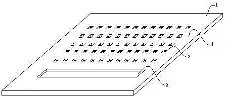
[0058] The invention discloses a manufacturing process of a step formwork.

[0059] Its technological process is as follows:

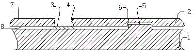
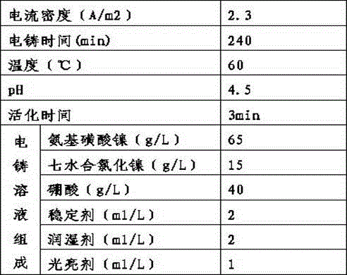
[0060] Electroforming the first electroforming layer: core mold treatment → pretreatment (degreasing, pickling, sandblasting) → film 1 → exposure 1 → single-sided development 1 → electroforming 1 → film fading → peeling;

[0061] The down step of etching the PCB surface: electroforming layer double-sided film → PCB surface exposure → PCB surface development → PCB surface etching → film fading → subsequent proces...


PUM


Abstract

A production process for a step stencil. The production process flow is as follows: electroforming a first electroformed layer: core mold treatment->pre-treatment (degreasing, pickling and sandblasting)->film mounting 1->exposure 1->single sided development 1-> electroforming 1->film stripping->mold stripping; and etching down steps on a PCB surface: double sided film mounting on the electroformed layer->PCB surface exposure->PCB surface development->PCB surface etching ->film stripping->follow-up treatment (degreasing and pickling). According to the stencil obtained by using the process, the PCB surface has a down step area, a plane area has pattern openings, and the down step area has no openings. The pure electroforming process of the invention solves the following technical problems: the PCB surface of the produced electroformed stencil has down steps; the produced entire electroformed stencil has smooth opening hole walls, no undesirable phenomena such as blurs and diffusion coating, good surface quality, no undesirable defects such as pinholes and pittings; the stencil thickness uniformity COV is less than 10%; and the stencil surface is in first grade brightness, with uniform brightness in the down step area after etching.

Description

technical field [0001] The invention relates to a manufacturing process of a step template, which belongs to the field of material manufacturing and processing, and specifically relates to a PCB surface in the field of PCB manufacturing with a down step step area and a planar area with a graphic opening. The manufacturing process of the printing mask plate with no pattern opening in the area. Background technique [0002] With the pursuit of miniaturization of electronic products, the perforated plug-in components used before can no longer be reduced; the functions of electronic products are more complete, and the integrated circuits (ICs) used can no longer perforate components, especially large-scale and highly integrated ICs, which have to use surface SMT components, so the stencil printing process has developed rapidly in the electronics manufacturing industry, and SMT printing is a typical example. The procurement of templates is not only the first step in the SMT asse...

Claims


Application Information

Patent Timeline
Patent Type & Authority Patents(China)
IPC IPC(8): B41C1/12B41N1/04B41N3/03G03F7/00
Inventor 魏志凌高小平王峰孙倩
Owner KUN SHAN POWER STENCIL
Why Eureka
Try Eureka