PCB engineering problem contrastive analysis and PCB engineering problem contrastive analysis result sending method and device

A comparative analysis, 1.PCB technology, applied in the field of network electronic technology applications, can solve problems such as poor communication, low communication efficiency, and inability to communicate intuitively, so as to achieve smooth communication and improve efficiency.

Inactive Publication Date: 2013-09-04
SHENZHEN PARTNER INFORMATION TECH
View PDF5 Cites 14 Cited by
  • Summary
  • Abstract
  • Description
  • Claims
  • Application Information

AI Technical Summary

Problems solved by technology

[0002] When existing customers need to print PCB boards, they need to send the Gerber file carrying the PCB board design information to the manufacturer. The manufacturer analyzes the Gerber file, evaluates the circuit design and production parameters obtained by the analysis, and judges the feasibility of production. If the evalu

Method used


Image

  • PCB engineering problem contrastive analysis and PCB engineering problem contrastive analysis result sending method and device
  • PCB engineering problem contrastive analysis and PCB engineering problem contrastive analysis result sending method and device
  • PCB engineering problem contrastive analysis and PCB engineering problem contrastive analysis result sending method and device

Examples


Embodiment Construction

[0048] The technical solutions of the present invention will be further described below in conjunction with the accompanying drawings and through specific implementation methods.

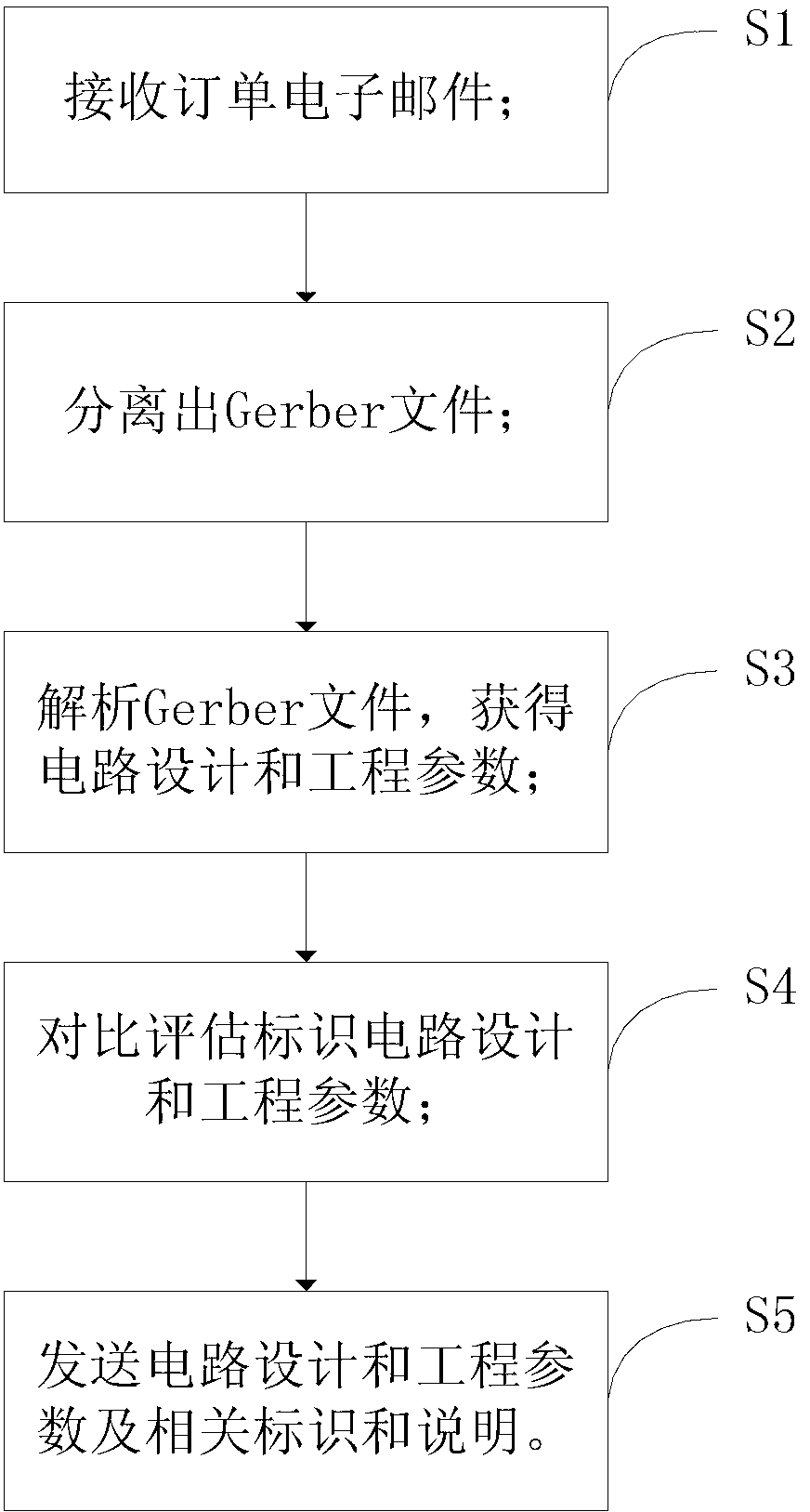
[0049] figure 1 It is the flow chart of the first embodiment of the method for comparative analysis of PCB engineering problems and the sending of results thereof in the present invention. As shown in the figure, the method includes:

[0050] Step S1: Receive the PCB order email carrying the Gerber file;

[0051] Step S2: separating the Gerber file from the PCB order email;

[0052] Step S3: analyzing the separated Gerber file to obtain the circuit design and engineering parameters of the PCB board carried in the Gerber file;

[0053] Step S4: Automatically compare the analyzed circuit design and engineering parameters with the circuit design and engineering parameters in the preset circuit database and production process database. At the technical level, the wrong circuit design is automatically...


PUM


Abstract

The invention discloses a PCB engineering problem contrastive analysis and PCB engineering problem contrastive analysis result sending method and device. The method comprises the steps of receiving PCB order form E-mails carrying Gerber files, extracting the Gerber files from the PCB order form E-mails, analyzing the extracted Gerber files, obtaining PCB circuit design and engineering parameters carried in the Gerber files, conducting comparison between the analytical circuit design and engineering parameters and preset circuit design and engineering parameters, when the analytical circuit design and engineering parameters are wrong or cannot reach a manufacturing technique level, marking relevant circuit design, giving out problem descriptions and modification references, and sending the analytical circuit design and engineering parameters, marks on the relevant circuit design, the problem descriptions and the modification references to an outbox of the PCB order form E-mails. The method strengthens convenience of communication between a client and a manufacturer in a circuit board printing process, and improves communication efficiency.

Description

technical field [0001] The invention relates to the application field of network electronic technology, in particular to a method and a device for comparative analysis of PCB engineering problems and sending results thereof. Background technique [0002] When existing customers need to print PCB boards, they need to send the Gerber file carrying the PCB board design information to the manufacturer. The manufacturer analyzes the Gerber file, evaluates the circuit design and production parameters obtained by the analysis, and judges the feasibility of production. If the evaluation shows that there is a problem, it is necessary to communicate separately by e-mail or telephone, and because the error in the circuit design or the deviation of the production parameter cannot be communicated intuitively during the communication process, there is a problem of poor communication and low communication efficiency. Contents of the invention [0003] The present invention provides a met...

Claims


Application Information

Patent Timeline
IPC IPC(8): G06Q10/10G06F17/30
CPCG06Q10/10
Inventor 曾波
Owner SHENZHEN PARTNER INFORMATION TECH
Why Eureka
Try Eureka