Input device and method of manufacturing the same

An input device, non-input technology, applied in the input/output process of data processing, instruments, electrical digital data processing, etc., can solve the problems of increasing wiring resistance deviation, disconnection, etc. The effect of reducing the probability of disconnection

Active Publication Date: 2013-09-25
ALPS ALPINE CO LTD
View PDF6 Cites 0 Cited by
  • Summary
  • Abstract
  • Description
  • Claims
  • Application Information

AI Technical Summary

Problems solved by technology

In addition, there is a problem that the variation in the wiring resistance of each wiring layer becomes large.
[0007] In addition, in the invention described in Patent Document 2, the longer the length dimension of the wiring layer, the narrower the wiring width is, so the problem of disconnection is more likely to occur, and the variation in wiring resistance further increases.

Method used


Image

  • Input device and method of manufacturing the same
  • Input device and method of manufacturing the same
  • Input device and method of manufacturing the same

Examples


Embodiment Construction

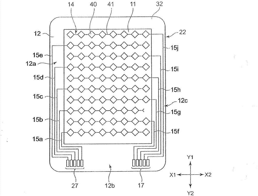
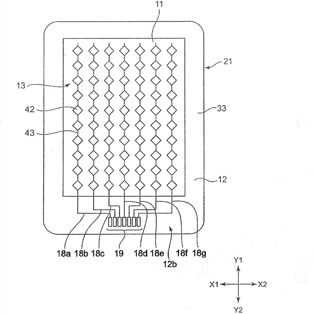
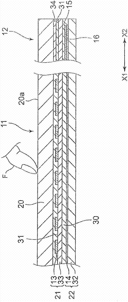
[0050] figure 1 It is a plan view of the lower substrate of the capacitive input device (touch panel) of this embodiment, figure 2 is the top view of the upper substrate, image 3 It is a partial vertical cross-sectional view of the input device in this embodiment when it is cut in the X1-X2 direction, Figure 4 (a) is a partial enlarged plan view of the wiring layer in this embodiment, Figure 4 (b) means Figure 4 A schematic diagram of the wiring width of the wiring extension part of each wiring layer shown in (a), Figure 4(c) is to show that with Figure 4 (b) Schematic diagrams of wiring widths in different systems.

[0051] figure 1 , image 3 The lower substrate 22 is shown having a lower substrate 32 and a plurality of lower electrode layers 14 formed on the surface of the lower substrate 32 . Each lower electrode layer 14 is formed in the input region (sensor region) 11 .

[0052] Such as figure 1 As shown, each lower electrode layer 14 is in the form o...


PUM


Abstract

The invention provides an input device and a method of manufacturing the same. A wiring layer comprises a plurality of wires provided with connecting end parts which are configured at a connection position connected with the end part of an electrode layer and; and wiring extension parts which are pulled out from the connecting end parts. Each connecting end is the widest wiring part in each wiring layer, when the two orthogonal directions in a plane is set as a first direction and a second direction, the wiring extension parts within a plurality of said wiring layers are extended respectively in the second direction in a state where there are a gaps in the first direction on the non-input area side on the same side as the input area, while the wire width of each of the wiring extension part is provided in proximity in a row arrangement in the first direction, and is such that the less the number of areas of wiring layers, the larger the wire width.

Description

[0001] This application is a divisional application, the application number of its parent application: 201180018663.0, the filing date: 2011.07.06, the title of the invention: input device and its manufacturing method. technical field [0002] The present invention relates to an input device configured by extending and forming a plurality of wiring layers in a non-input area located outside the input area, and particularly relates to the structure of the wiring layers. Background technique [0003] The configuration of the input device (touch panel) is disclosed in the following patent documents 1 and 2. FIG. A plurality of electrode layers are arranged in the input area of ​​the input device. In addition, when the operator operates the input area with a finger or the like, the operation position can be detected by a change in electrostatic capacitance or the like. A wiring layer electrically connected to each electrode layer is formed in a non-input area outside the input ...

Claims


Application Information

Patent Timeline
Patent Type & Authority Applications(China)
IPC IPC(8): G06F3/044G06F3/041
CPCG06F3/0445G06F3/0446G06F3/041G06F3/044
Inventor 高桥亨佐藤清佐佐木义人桥本秀幸尾崎恭辅
Owner ALPS ALPINE CO LTD
Why Eureka
Try Eureka