LED display screen with same-color chips arrayed diagonally and method for reusing pixels

An LED display, pixel multiplexing technology, applied in static indicators, instruments, identification devices, etc., can solve the problems of difficult circuit board wiring, blurred images, etc., to avoid blurred images, reduce wiring pressure, and route wiring. small space effect

Active Publication Date: 2013-09-25
长春瑞隆达电子技术有限公司
View PDF6 Cites 21 Cited by
  • Summary
  • Abstract
  • Description
  • Claims
  • Application Information

AI Technical Summary

Problems solved by technology

The common disadvantage of these solutions is that due to the mixed arrangement of red, green and blue LED lights, the lights of each color are not on the same line, which will bring great difficulties to the circuit board wiring for ultra-high-density displays.
In addition, for ultra-high-density LED displays, since the physical density of the LED die itself is already very high, the virtual pixel display of more than 10 times does not make much sense, and with the increase of the virtual multiple, the image will have a certain degree of blur

Method used


Image

  • LED display screen with same-color chips arrayed diagonally and method for reusing pixels
  • LED display screen with same-color chips arrayed diagonally and method for reusing pixels
  • LED display screen with same-color chips arrayed diagonally and method for reusing pixels

Examples


Embodiment 1

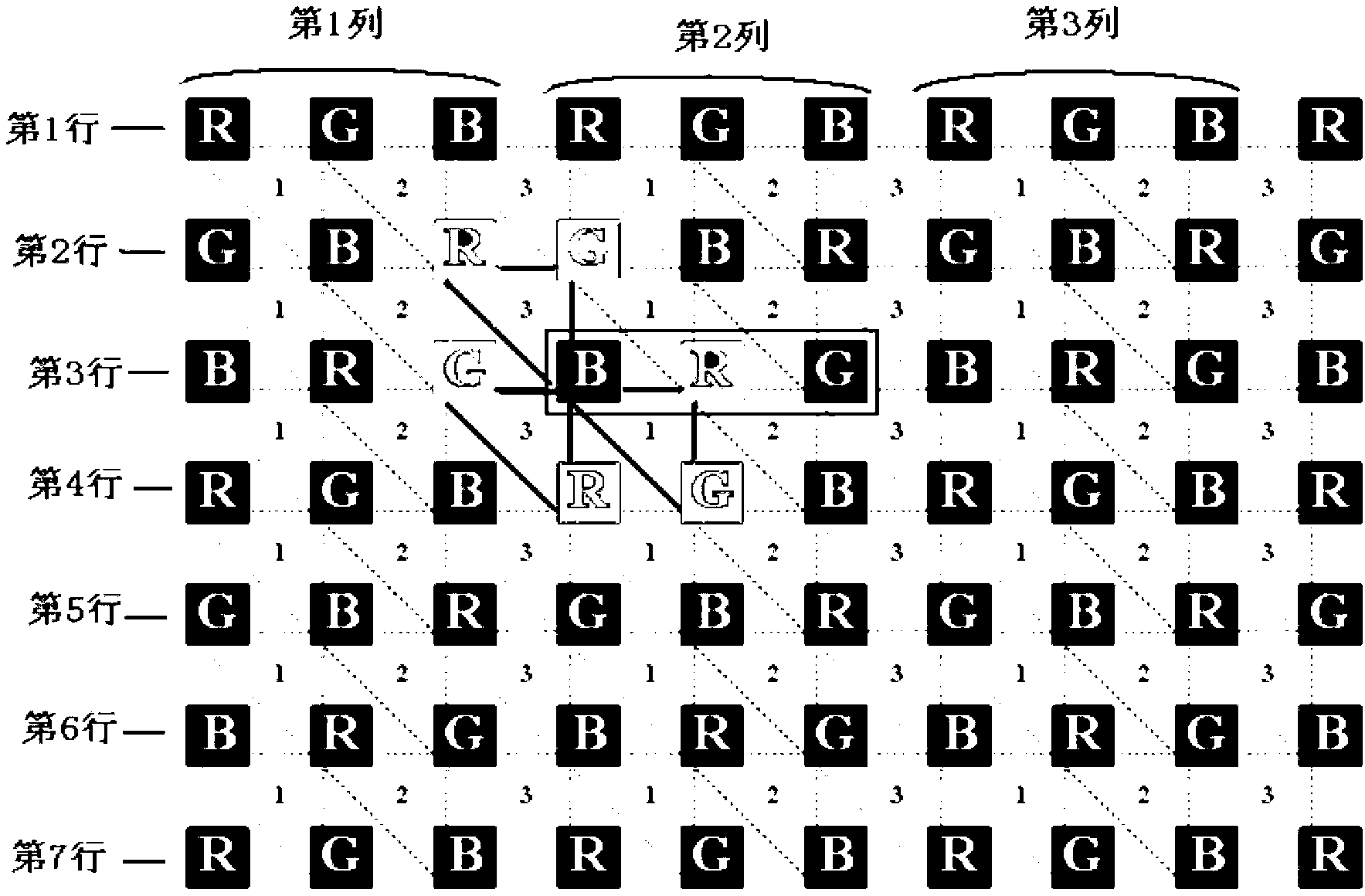
[0036] Such as figure 1 As shown, R, G, and B respectively represent the red, green, and blue primary color LED chips on the display screen. The three-primary-color LED chips on the circuit board are aligned vertically and horizontally, and are evenly spaced in the order of R, G, and B in the horizontal direction from left to right and vertically from top to bottom. The connecting line is a slanted line at 45 degrees. In the oblique direction of 135 degrees, in the order of R, G, and B, they are arranged obliquely in turn; a group of red, green, and blue primary-color LED chips horizontally or vertically form a physical pixel point. Except for the edge LED chips, each LED chip and its surroundings The six LED chips form three triangles containing red, green and blue primary color LED chips. The three triangles including red, green and blue primary color LED chips share the LED chip. For example, each blue LED chip B and its surrounding three green LED chips G and three red ...

Embodiment 2

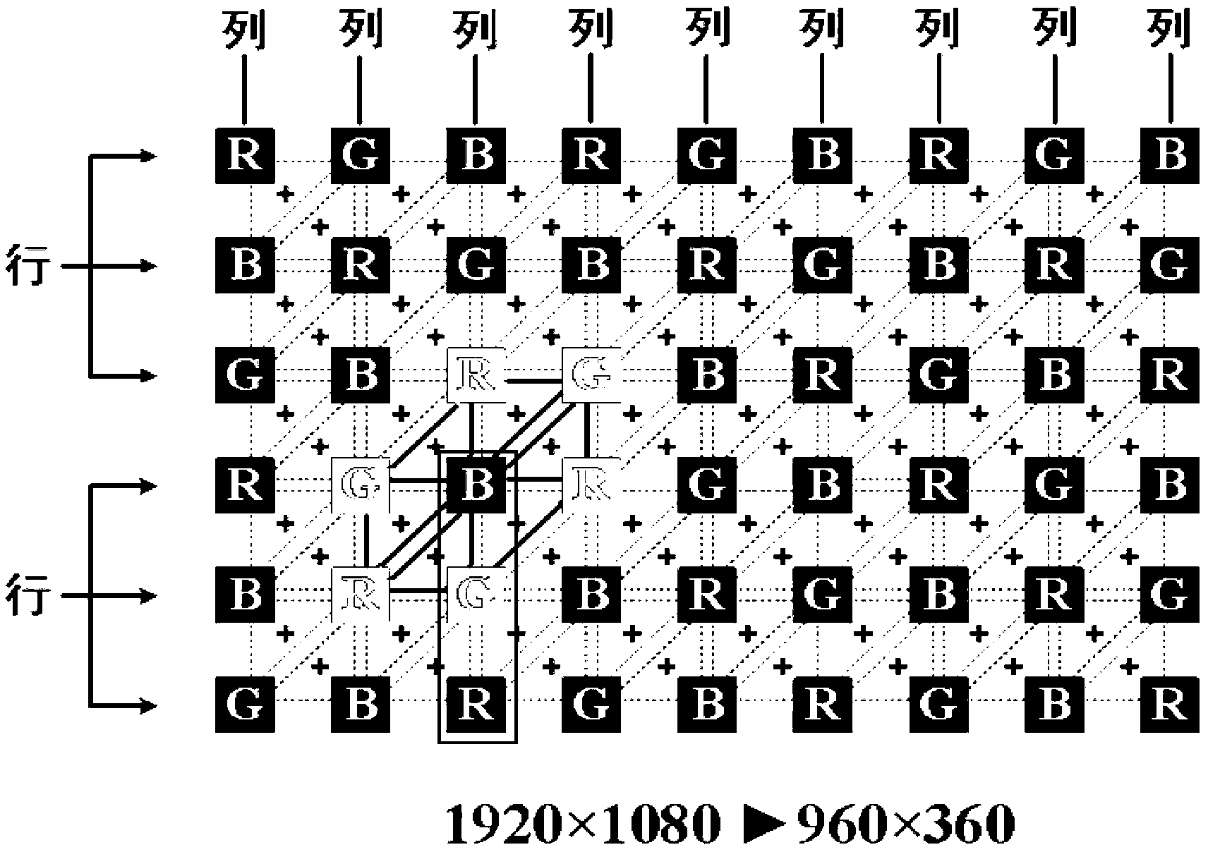
[0055] Such as figure 2 As shown, R, G, and B respectively represent the red, green, and blue primary color LED chips on the display screen. The three-primary-color LED chips on the circuit board are aligned vertically and horizontally. The horizontal spacing between the LED chips is not equal to the vertical spacing, and they are evenly spaced in the order of R, G, and B from left to right in the horizontal direction, and from top to bottom in the vertical direction. Arrange evenly at equal intervals in the order of R, B, and G. The connection lines of the LED chips of each primary color on the display screen are oblique lines. In the direction perpendicular to the oblique line, they are arranged diagonally in the order of R, B, and G; a group of red, green, and blue primary-color LED chips in the vertical direction form a physical pixel point. Except for the edge LED chips, each LED chip and its surroundings The six LED chips form six triangles including red, green and bl...

Embodiment 3

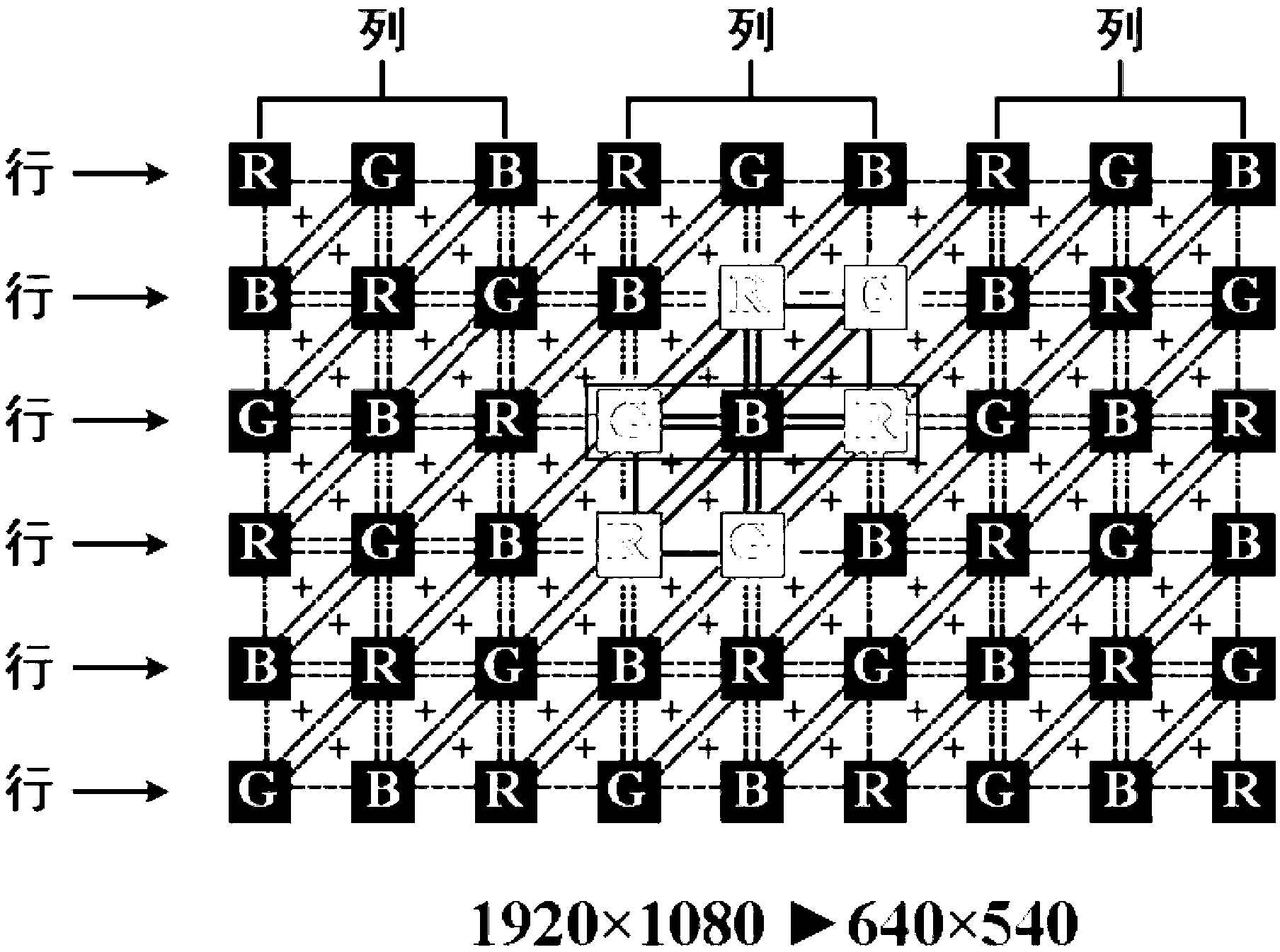
[0074] Such as image 3 As shown, R, G, and B respectively represent the red, green, and blue primary color LED chips on the display screen. The three-primary-color LED chips on the circuit board are aligned vertically and horizontally. The horizontal spacing between the LED chips is smaller than the vertical spacing, and they are evenly spaced in the order of R, G, and B from left to right in the horizontal direction. The order of R, B, and G is evenly spaced. The connection lines of the LED chips of each primary color on the display screen are oblique lines. In the direction perpendicular to the oblique line, they are arranged obliquely in the order of R, B, and G; a group of red, green, and blue primary color LED chips in the horizontal direction form a physical pixel point. Except for the edge LED chips, each LED chip and its surroundings The six LED chips form six triangles including red, green and blue primary color LED chips. Six triangles including red, green and bl...


PUM


Abstract

The invention relates to an LED display screen with same-color chips arrayed diagonally and a method for reusing pixels. The three-primary-color LED chips of the display screen are respectively transversely and longitudinally linearly arranged equidistantly, the same-primary-color LED chips are arranged to form diagonals, and the corresponding three-primary-color LED chips are equidistantly, sequentially, alternately and diagonally arranged in the direction perpendicular to each diagonal. The method for reusing the pixels includes corresponding to primary-color display data of an optional LED chip to primary-color display data of n adjacent pixels of an image source, adding the primary-color display data of the n adjacent pixels to obtain a sum, and dividing the sum by the number n to obtain display data of the LED chip; transmitting acquired display data of the various three-primary-color LED chips to the display screen via a scanning driving circuit so that the display data can be displayed on the display screen. The LED display screen and the method have the advantages that the circuit board wire arrangement pressure is effectively relieved, the production cost can be greatly lowered, the production efficiency is improved, and the LED display screen and the method are particularly applicable to ultrahigh-density LED display.

Description

technical field [0001] The invention belongs to the technical field of LED flat panel display, and relates to an LED display screen with diagonally arranged chips of the same color and a method for realizing pixel multiplexing by using the display screen. Background technique [0002] As a digital image display medium, the LED display can display the image information of the video image in real time. There are two key factors that affect the display effect of the LED display: one is the resolution of the LED display, that is, the pixel density per unit area, and the other is the display color and gray level of the display. In terms of display color and gray scale, the display color of the LED display has reached 256 levels at present, and the single-color gray scale resolution is 10-16bit. From the display level, the LED display has been able to meet the requirements as a digital display terminal. Improving display efficiency by increasing the physical resolution, that is,...

Claims


Application Information

Patent Timeline
Patent Type & Authority Applications(China)
IPC IPC(8): G09F9/33G09G3/32
Inventor 王瑞光邓意成陈宇田志辉
Owner 长春瑞隆达电子技术有限公司
Why Eureka
Try Eureka