Abnormal state detection method for optical indicating device
A technology of indicating device and abnormal state, applied in the direction of instrument, electrical digital data processing, and data processing input/output process, etc., can solve problems such as output, and achieve the effect of more resources, less calculation, and lower power consumption
- Summary
- Abstract
- Description
- Claims
- Application Information
AI Technical Summary
Problems solved by technology
Method used
Image

Examples
Embodiment Construction
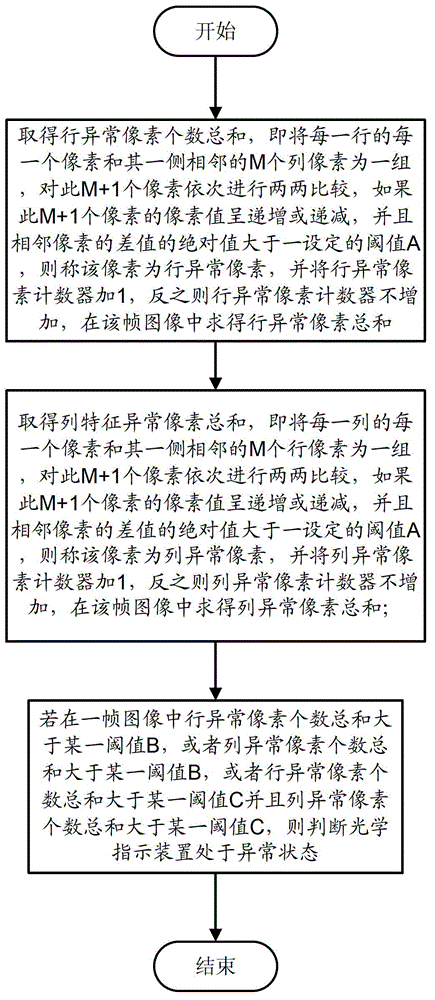
[0011] The abnormal state detection method of the optical indicating device of the present invention is applied to the optical indicating device. The optical indicating device is provided with an image sensor array, and the image sensor array samples an external frame image and outputs a pixel matrix corresponding to the image sensor array , the method includes the following steps:
[0012] (1) Obtain the sum of the number of abnormal pixels in the row, that is, each pixel in each row and the M adjacent column pixels on one side are grouped, and the M+1 pixels are compared in turn. If this M+ If the pixel value of one pixel is increasing or decreasing, and the absolute value of the difference between adjacent pixels is greater than a set threshold A, then the pixel is called a row abnormal pixel, and the row abnormal pixel counter is increased by 1, otherwise, the row abnormal pixel The abnormal pixel counter does not increase, and the sum of row abnormal pixels is obtained in...
PUM
 Abstract
Description
Claims
Application Information
 - R&D Engineer
- R&D Manager
- IP Professional
- Industry Leading Data Capabilities
- Powerful AI technology
- Patent DNA Extraction
Browse by: Latest US Patents, China's latest patents, Technical Efficacy Thesaurus, Application Domain, Technology Topic.
© 2024 PatSnap. All rights reserved.Legal|Privacy policy|Modern Slavery Act Transparency Statement|Sitemap