Supercharge Your Innovation With Domain-Expert AI Agents!

Multiple times programmable memory cell and method for forming same

A memory cell and active area technology, applied in the semiconductor field, can solve the problem of large chip area of ​​MTP memory cell

Active Publication Date: 2016-01-20
TAIWAN SEMICON MFG CO LTD
View PDF5 Cites 0 Cited by
  • Summary
  • Abstract
  • Description
  • Claims
  • Application Information

AI Technical Summary

Problems solved by technology

Therefore, the chip area occupied by the MTP memory cell is larger

Method used


Image

  • Multiple times programmable memory cell and method for forming same
  • Multiple times programmable memory cell and method for forming same
  • Multiple times programmable memory cell and method for forming same

Examples


Embodiment Construction

[0028] The making and using of embodiments of the present disclosure are discussed in detail below. It should be appreciated, however, that the embodiments provide many applicable inventive concepts that can be embodied in a wide variety of specific contexts. The specific embodiments discussed are exemplary, and do not limit the scope of the disclosure.

[0029] Multiple time programmable (MTP) memory cells and methods of forming the same are provided according to various exemplary embodiments. Intermediate stages in the formation of the MTP memory cell are shown. Variations of the embodiments are discussed. The same reference numerals are used to designate the same elements throughout the drawings and exemplary embodiments.

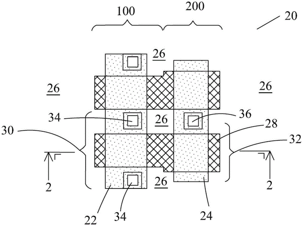
[0030] figure 1 The layout of a portion of the MTP memory cell 20 is shown. The portion shown includes active regions 22 and 24 . Active regions 22 and 24 are portions of semiconductor regions isolated from each other by isolation regions 26 . Acc...


PUM


Abstract

A device includes an active region and a coupling capacitor. The capacitor includes a first floating gate, an upper plate of the capacitor serving as a coupling capacitor, and a doped semiconductor region, a lower plate of the capacitor serving as a coupling capacitor. The doped semiconductor region includes a surface portion located at the surface of the active region, and a sidewall portion lower than the bottom surface of the surface portion. The sidewall portion is located on the sidewall of the active region. A capacitor insulator is disposed between the capacitor upper plate and the capacitor lower plate. The capacitor insulator includes an upper portion, and a sidewall portion lower than a bottom surface of the upper portion. The invention also provides the multi-time programmable storage unit and its forming method.

Description

technical field [0001] The present invention generally relates to the field of semiconductor technology, and more specifically, relates to multiple times programmable memory cells. Background technique [0002] A multiple-time programmable (Multiple-Time Programming, MTP) storage unit can retain information stored in the storage unit even if the power is cut off. Typically, to form an MTP memory cell, a standard complementary metal oxide semiconductor (CMOS) based logic process is used as a starting basis. Additional process steps may be incorporated into the logic process flow to form the MTP memory cell. Examples of such additional process steps include second polysilicon deposition, junction dopant optimization, and the like. MTP memory cells generally require larger capacitors to improve the programming efficiency of the MTP memory cells. Therefore, the chip area occupied by the MTP storage unit is large. Contents of the invention [0003] In order to solve the def...

Claims


Application Information

Patent Timeline
Patent Type & Authority Patents(China)
IPC IPC(8): H01L27/115H01L21/8247G11C16/04
CPCH01L28/60G11C16/0408H01L29/40114H01L28/40H10B41/60H10B41/30H10B41/00H01L21/76205H01L21/76213H01L21/76237H01L29/42324H01L29/66825H01L21/0223H01L21/265H01L21/30604H01L21/32055H01L21/76224
Inventor 傅景鸿柯钧耀简铎欣许庭祯
Owner TAIWAN SEMICON MFG CO LTD
Features
  • R&D
  • Intellectual Property
  • Life Sciences
  • Materials
  • Tech Scout
  • Unparalleled Data Quality
  • Higher Quality Content
  • 60% Fewer Hallucinations
Learn More