Programmable resistance memory device

Active Publication Date: 2006-11-30
KIOXIA CORP
View PDF17 Cites 129 Cited by
  • Summary
  • Abstract
  • Description
  • Claims
  • Application Information

AI Technical Summary

Benefits of technology

[0005] A programmable resistance memory device accor

Problems solved by technology

However, there has not been proposed a detailed configuration of a cell array and a read/write circuit thereof.
In order to achieve a practical non-volatile memory with a high density and a high performance, how to combine

Method used


Image

  • Programmable resistance memory device
  • Programmable resistance memory device
  • Programmable resistance memory device

Examples


Embodiment Construction

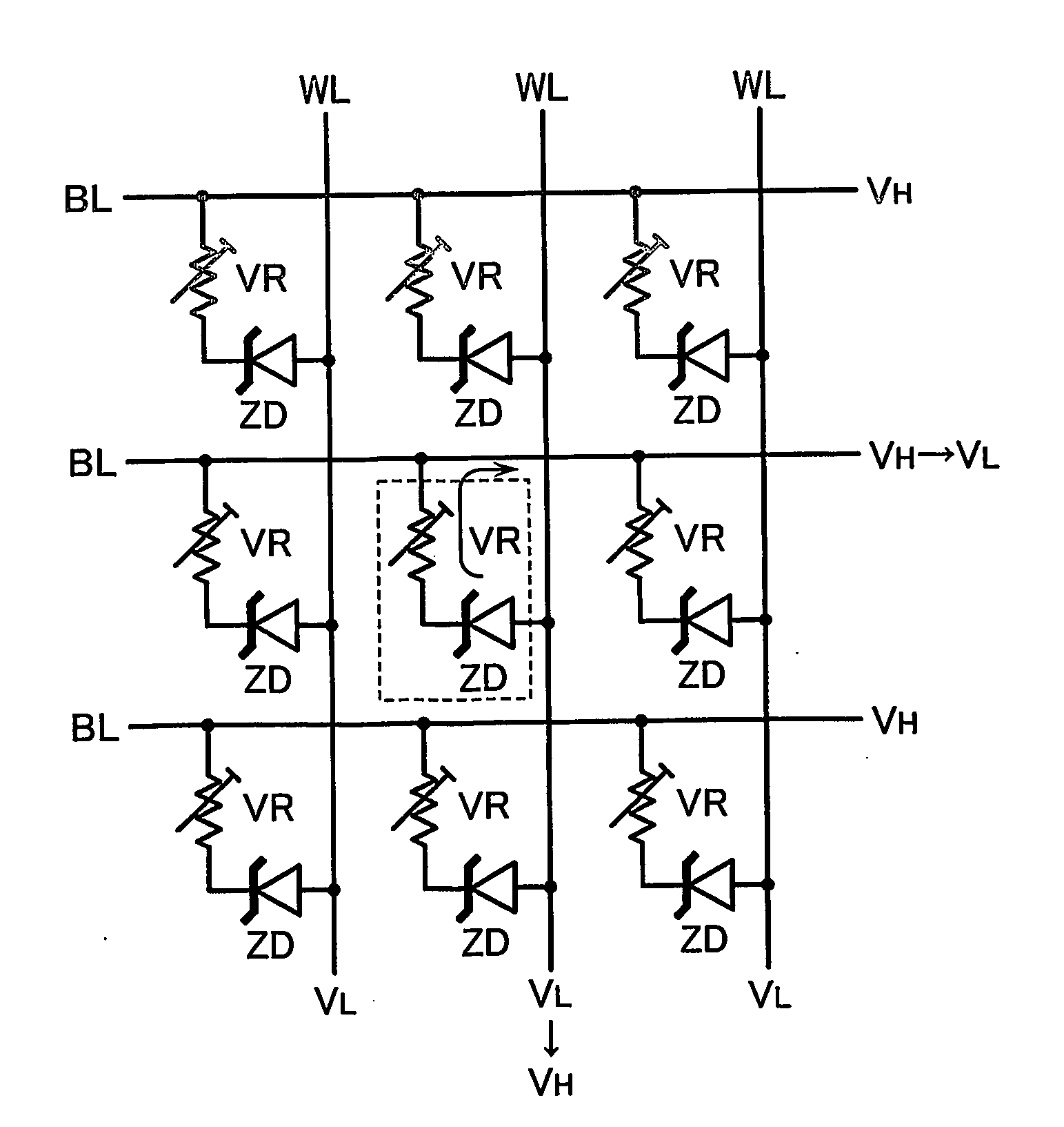
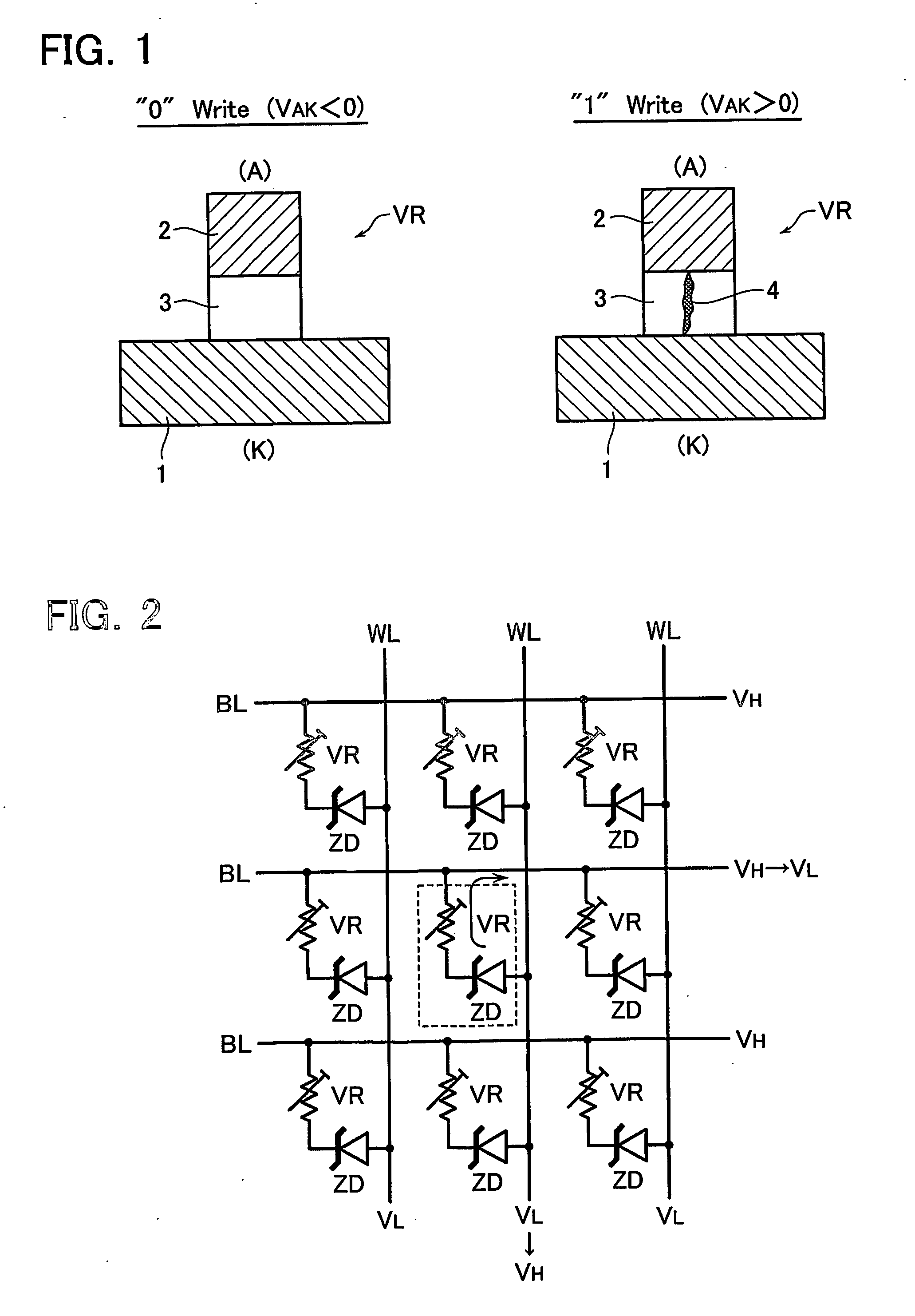
[0037]FIG. 1 shows a principle configuration of a programmable resistance (variable resistance) VR used in the present invention. The programmable resistance VR is formed of a resistance film 3 serving as a memory material, and cathode and anode electrodes 1 and 2 sandwiching the resistance film 3. The resistance film 3 is, for example, an ion conductor (solid electrolyte) formed of a chalcogenide containing metal ions such as silver, cupper and the like. For example, Ge—S, Ge—Se and the like may be used as the chalcogenide. In the case that the resistance film 3 is formed of the above-described chalcogenide, the electrodes 1, 2 are formed containing silver therein.

[0038] The resistance film 3 stores, for example, a high resistance state as a data “0” and a low resistance state as a data “1”. In this programmable resistance VR, apply a positive anode-cathode voltage (VAK>0) that is over a threshold value, and a data “1” will be written. Apply a negative anode-cathode voltage (VAKAK...


PUM


Abstract

programmable resistance memory device includes: a semiconductor substrate; at least one cell array, in which memory cells are arranged, formed above the semiconductor substrate, each the memory cell having a stack structure of a programmable resistance element and an access element, the programmable resistance element storing a high resistance state or a low resistance state determined due to the polarity of voltage application in a non-volatile manner, the access element having such a resistance value in an off-state in a certain voltage range that is ten times or more as high as that in a select state; and a read/write circuit formed on the semiconductor substrate as underlying the cell array for data reading and data writing in communication with the cell array.

Description

TECHNICAL FIELD [0001] This invention relates to a programmable resistance memory device for storing a resistance state as data in a non-volatile manner, with a programmable resistance element which is switchable between a low resistance state and a high resistance state by reversing the polarity of voltage application. BACKGROUND ART [0002] Recently, there have been proposed some memory devices having programmable resistance elements. One of such the memory devices is known as a phase change memory which uses phase transition between an amorphous state and a crystalline state of a memory material (for example, U.S. Pat. No. 6,314,014B1). In such the phase change memory device, by controlling the current of a chalcogenide cell, reversible switching may be performed between a crystalline state (i.e. low resistance state) and an amorphous state (i.e. high resistance state). Apply a large current to a cell so as to cause the cell chalcogenide to be melted, then rapidly cool down it, an...

Claims


Application Information

Patent Timeline
IPC IPC(8): G11C17/00G11C11/36G11C13/02H01L27/24
CPCG11C13/0011H01L45/1683G11C2013/009G11C2213/15G11C2213/71G11C2213/72H01L27/2409H01L27/2436H01L27/2481H01L45/085H01L45/1233H01L45/141H01L45/142H01L45/143H01L45/1641H01L45/1675G11C13/0069H10B63/20H10B63/84H10N70/245H10N70/826H10N70/8822H10N70/8825
Inventor TODA, HARUKI
Owner KIOXIA CORP
Why Eureka
Try Eureka