Supercharge Your Innovation With Domain-Expert AI Agents!

Method for making pixel definition layer

A technology for defining a pixel definition layer and a manufacturing method, which is applied in the directions of copying/marking method, semiconductor/solid-state device manufacturing, printing, etc., and can solve problems such as poor display and overflow

Active Publication Date: 2016-03-23
BOE TECH GRP CO LTD
View PDF5 Cites 0 Cited by
  • Summary
  • Abstract
  • Description
  • Claims
  • Application Information

AI Technical Summary

Problems solved by technology

[0004] However, in the actual inkjet printing process, the inkjet printing ink may overflow a small amount, and it will overflow in the adjacent pixel area, resulting in poor display

Method used


Image

  • Method for making pixel definition layer
  • Method for making pixel definition layer
  • Method for making pixel definition layer

Examples


Embodiment Construction

[0049] The following will clearly and completely describe the technical solutions in the embodiments of the present invention with reference to the accompanying drawings in the embodiments of the present invention. Obviously, the described embodiments are only some, not all, embodiments of the present invention.

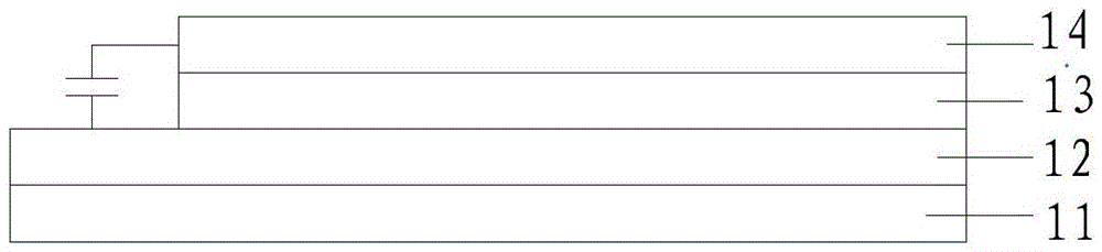
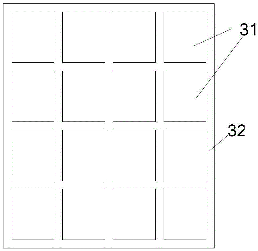
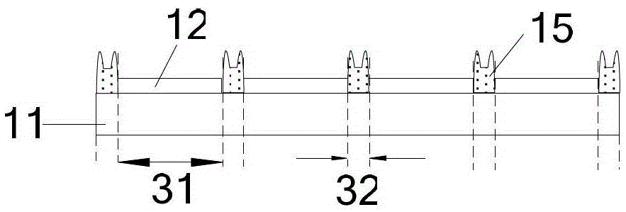
[0050] An embodiment of the present invention provides a pixel defining layer, the pixel defining layer includes a pixel partition wall pattern, and the upper surface of the pixel partition wall has a depression. Such as image 3 As shown, the upper surface of the pixel separation wall 15 is inwardly recessed at the middle part to form a groove.

[0051] It should be noted that in all the embodiments of the present invention, the definitions of "layer" and "pattern" and the relationship between them need to be clarified. Wherein, "layer" refers to a layer of thin film made of a certain material on a substrate by deposition or other processes, which includes a "patte...


PUM

PropertyMeasurementUnit
boiling pointaaaaaaaaaa

Abstract

The invention provides a method for manufacturing a pixel defining layer, relates to the field of display technology, and solves the problem of poor display caused by a small amount of ink overflowing to adjacent pixel regions in the existing inkjet printing. The present invention provides a pixel defining layer, wherein the pixel defining layer includes a pixel partition wall pattern, and the upper surface of the pixel partition wall has a depression.

Description

technical field [0001] The invention relates to the field of display technology, in particular to a method for manufacturing a pixel defining layer. Background technique [0002] Inkjet printing technology is one of the main technologies used in modern office printing. In recent years, researchers have begun to try to apply inkjet printing technology to the preparation of planar functional materials, such as the preparation of polymer conductive films, the preparation of color organic light-emitting diodes, the preparation of Thin film semiconductor devices, etc. [0003] Existing (OrganicLightEmittingDiode, Organic Light Emitting Diode) display device, such as figure 1 As shown, the OLED display substrate includes a base substrate 11 , an anode electrode layer 12 disposed on the base substrate 11 , a light emitting function layer 13 , and a cathode electrode layer 14 . The display device includes a plurality of pixel regions 31 and non-pixel regions 32, such as figure 2...

Claims


Application Information

Patent Timeline
Patent Type & Authority Patents(China)
IPC IPC(8): H01L27/32H01L21/77B41M5/00
CPCH10K59/122H10K59/173
Inventor 侯文军刘则
Owner BOE TECH GRP CO LTD
Features
  • R&D
  • Intellectual Property
  • Life Sciences
  • Materials
  • Tech Scout
  • Unparalleled Data Quality
  • Higher Quality Content
  • 60% Fewer Hallucinations
Learn More